

Semiconductor Industry in India: Incentives, Key Players, and the 2026 Outlook



Explore the semiconductor industry in India in 2026: ISM 2.0 incentives, approved projects, Tata and Micron investments, execution risks, and outlook.
Semiconductor Industry in India: Incentives, Key Players, and the 2026 Outlook
Did you know that the Indian central government is prepared to underwrite 50 percent of project costs for semiconductor fabrication plants through a $10 billion flagship fiscal incentive package—an offer so generous that it rivals subsidy regimes in Taiwan, South Korea, and the United States? This is not aspirational planning locked in a policy document; it is a live, capital-heavy commitment designed to move India from a chip-importing nation to a credible global manufacturing hub before the decade’s midpoint. As geopolitical tensions reshape supply chains and the world races to secure silicon sovereignty, the Semiconductor Industry in India has become one of the most closely watched investment theaters on the planet.
Why 2026 Is India's Semiconductor Inflection Point
For years, India’s relationship with semiconductors was defined by an uncomfortable paradox: the country produced world-class chip designers and hosted the research centers of nearly every major global player, yet it manufactured almost negligible volumes of silicon domestically. Smartphones, data centers, automobiles, and defense systems all relied on imported chips, leaving the economy exposed to supply shocks and currency fluctuations. That narrative is now shifting, driven by a trifecta of government incentives, foreign direct investment, and strategic urgency.
At the heart of this transformation is the India Semiconductor Mission (ISM), which functions as the coordinating nerve center for a suite of aggressive subsidy programs. The Production-Linked Incentive (PLI) Scheme targets capital-intensive fabrication and packaging facilities, offering tiered disbursements that improve unit economics for players willing to build on Indian soil. Complementing this is the Design Linked Incentive (DLI) Scheme, which the Press Information Bureau notes provides incentives of 6% to 4% of net sales turnover over five years, alongside infrastructure support at multiple stages of development. Unlike generic R&D subsidies, the DLI is calibrated to shepherd semiconductor designs from specification to tape-out, ensuring that Indian companies capture value upstream rather than merely providing back-end verification services.
The fiscal arithmetic is compelling. A 2024 report from the Information Technology and Innovation Foundation (ITIF) confirms that New Delhi’s strategy revolves around a $10 billion match package, where the central government splits project costs halfway with private investors. This level of risk-sharing is critical because a single advanced fab can cost upwards of $5 billion to $20 billion, and few firms are willing to shoulder that exposure alone. Beyond fabs, states like Uttar Pradesh are aggressively marketing their investment climates for ATMP—Assembly, Testing, Marking, and Packaging—facilities, recognizing that packaging is where India can achieve near-term scale while cutting-edge logic manufacturing matures.
Investors are responding. Invest India explicitly frames the country’s semiconductor sector as a high-growth investment opportunity, citing increasing global demand and robust government backing as dual catalysts. With investments in fabs and chip packaging units no longer theoretical, India’s ecosystem is beginning to resemble the integrated verticals seen in Vietnam and Malaysia—albeit with a far larger domestic consumption base and a deeper bench of electrical engineers.
What This Report Will Uncover
By 2026, the decisions made in New Delhi’s boardrooms and state industrial corridors will determine whether India becomes a meaningful node in the global silicon supply chain or remains a design outpost for foreign fabs. The next three years are pivotal: project timelines for mature-node facilities typically run 24 to 36 months, talent pipelines must scale rapidly, and ancillary ecosystems—from specialty gases to cleanroom logistics—must localize in parallel.
In the sections that follow, we will provide a comprehensive analysis of:
- The Incentive Architecture — A detailed breakdown of how the PLI and DLI schemes interact, who qualifies, and how the 50 percent central government cost-share unlocks returns for both domestic conglomerates and multinationals.
- The Key Players — From global chipmakers scouting ATMP locations to Indian industrial houses betting on indigenous fabs and design startups, we map the entities actually moving dirt and hiring talent.
- The 2026 Outlook — A reality-check on infrastructure readiness, water and power requirements, talent density, and geopolitical tailwinds that will dictate whether India can mirror East Asian manufacturing discipline—or carve out a distinct niche in mature-node and compound semiconductors.
As artificial intelligence permeates every layer of the digital economy, the demand for localized, secure compute only intensifies. Platforms like CallMissed—which run AI voice agents, multilingual speech models, and LLM inference stacks—depend on this underlying silicon security, illustrating why a domestic semiconductor base matters not just to hardware manufacturers, but to India’s entire software and AI services ecosystem. The blueprint is drafted. The subsidies are live. The only question remaining is whether execution can match ambition before 2026.
Introduction

The Semiconductor industry in India has moved from policy design to project execution. As of July 2026, the country is building capabilities across wafer fabrication, chip design, and Assembly, Testing, Marking, and Packaging (ATMP), also known internationally as outsourced semiconductor assembly and test (OSAT).
According to India’s Press Information Bureau (PIB), 10 semiconductor projects with a combined investment of approximately ₹1.60 lakh crore have been approved under the India Semiconductor Mission. These projects represent substantial commitments, but approvals and announced investments should not be confused with completed factories or commercial-scale output. Timely construction, technology transfer, customer qualification, and production ramp-ups will determine the program’s results.
India Semiconductor Mission 2.0
The next policy phase is India Semiconductor Mission 2.0. PIB states that the Union Budget for FY 2026-27 includes a ₹1,000 crore provision, with an emphasis on industry-led research and training centres. This expands the mission’s focus beyond subsidizing factories to strengthening the research, skills, and institutional infrastructure required for a durable semiconductor ecosystem.
The policy direction matters because the Semiconductor industry in India cannot rely on capital incentives alone. Fabs require specialized engineers, uninterrupted power, large volumes of high-quality water, dependable suppliers, process expertise, and long-term customer relationships. Research partnerships and practical training centres can help address these constraints, provided their programs remain aligned with industry requirements.
The Ecosystem Taking Shape
India’s strategy covers several connected parts of the semiconductor value chain:
- Wafer fabrication: Large projects are intended to establish domestic manufacturing capacity for chips used in automotive, industrial, communications, consumer, and power applications.
- Chip design: India already hosts a significant engineering and semiconductor design workforce. The Design Linked Incentive framework seeks to help Indian companies convert design talent into commercially owned products and intellectual property.
- ATMP and OSAT: Packaging, assembly, and testing projects offer a practical route into semiconductor manufacturing while supporting increasingly important advanced-packaging capabilities.
- Research and skills: Mission 2.0’s focus on industry-led research and training is designed to build the technical workforce and applied knowledge needed to operate these facilities.
- Supply-chain development: Chemicals, gases, equipment maintenance, substrates, logistics, and cleanroom services must develop alongside headline manufacturing projects.
The emerging list of key participants includes Tata Electronics, Micron Technology, CG Semi, Kaynes Semicon, and the HCL-Foxconn venture, alongside design startups, global technology partners, state governments, and specialist suppliers. Their projects differ in scale, technology, and place within the value chain, making it important to assess each on its actual scope rather than treating every announcement as a new chip fab.
What This Guide Covers
This guide explains how the Semiconductor industry in India is developing and where execution still matters. Readers will learn:
- How central and state incentives support fabs, design companies, and ATMP/OSAT facilities
- Which approved projects and key players are shaping the market
- Why packaging and mature-node manufacturing are important to India’s strategy
- How India Semiconductor Mission 2.0 changes the policy emphasis
- Which risks—skills, infrastructure, technology access, costs, and production ramp-ups—could slow progress
The central question for the Semiconductor industry in India is no longer whether policy support exists. It is whether approved projects can become competitive, reliable operations connected to domestic and global customers.
Background & Context: From Import Reliance to Atmanirbhar Chips

For much of its history, the semiconductor industry in India was built around design rather than manufacturing. Global chip companies established large engineering centers in Bengaluru, Hyderabad, Noida, Pune, and Chennai. Indian teams worked on processor architecture, verification, embedded software, and system design.
The physical chips, however, were usually made elsewhere. India depended heavily on foundries in Taiwan, South Korea, China, the United States, and other manufacturing hubs. It also relied on overseas facilities for assembly, testing, marking, and packaging.
India did have strategic semiconductor capabilities, including the government-owned Semiconductor Laboratory in Mohali. But it lacked the high-volume commercial fabs and packaging network needed to support its growing electronics market. In practical terms, India contributed engineering talent while importing most of the finished silicon used in smartphones, vehicles, telecom equipment, industrial systems, and defense electronics.
Why the Import Model Became a Strategic Risk
The design-and-import model worked while global supply chains remained predictable. The disruption that began in 2020 exposed its weaknesses.
Pandemic-related shutdowns, logistics bottlenecks, and sudden changes in electronics demand contributed to a worldwide chip shortage. Indian automakers and electronics manufacturers faced longer lead times and limited bargaining power when overseas suppliers allocated scarce production.
Geopolitical tensions added another concern. A large share of global foundry capacity is concentrated in East Asia, while advanced semiconductor equipment and technology are increasingly affected by export controls. Chips were no longer viewed only as commercial inputs. They had become critical to economic security, digital infrastructure, and defense readiness.
These shocks strengthened the case for domestic capacity. The goal was not immediate self-sufficiency across every chip category. That would be unrealistic given the scale and specialization of the global industry. Instead, India began building selected capabilities in fabrication, mature-node chips, compound semiconductors, packaging, and domestic intellectual property.
The India Semiconductor Mission Changes the Model
In 2021, the Union government approved the Semicon India Programme with an outlay of ₹76,000 crore—widely described at the time as roughly $10 billion. The India Semiconductor Mission was established as the coordinating institution for implementing the program.
The policy architecture covers three important parts of the value chain:
- Semiconductor and display fabs: Eligible projects can receive central fiscal support equal to 50% of project cost on a pari-passu basis, subject to approval and scheme conditions.
- Compound semiconductors and packaging: Separate support is available for compound semiconductor, silicon photonics, sensor, discrete semiconductor, and ATMP/OSAT facilities.
- Chip design: The Design Linked Incentive scheme supports Indian companies developing semiconductor designs and intellectual property.
This distinction matters. Fab incentives offset the extraordinary cost of manufacturing infrastructure. Packaging support helps create a downstream production ecosystem. Design incentives build on skills India already possesses.
Electronics Production-Linked Incentive schemes also contribute to the broader investment environment by expanding domestic device manufacturing and, therefore, potential chip demand. They should not be confused with the fiscal support specifically approved for semiconductor fabs.
From Fabless Talent to Indian-Owned IP
The Design Linked Incentive, or DLI, scheme addresses a long-standing gap. India has a large semiconductor engineering workforce, but much of its work has historically been performed for multinational companies rather than Indian product businesses.
DLI assistance includes reimbursement for eligible design expenditure and a deployment-linked incentive based on net sales, subject to program limits and eligibility rules. The scheme also provides access to design tools, prototyping resources, and related infrastructure through the ChipIN Centre.
The intended shift is from design services to product ownership. A successful Indian fabless company can create a chip, retain its intellectual property, arrange fabrication through a foundry, and sell the resulting product into automotive, industrial, telecom, consumer, or strategic markets. Domestic fabrication is not required for every such company, but a stronger local ecosystem can reduce development friction and improve supply-chain resilience.
Packaging Becomes the Practical Entry Point
Building a leading-edge fab is expensive, technically difficult, and dependent on highly specialized equipment, materials, water, power, and operating expertise. ATMP and OSAT facilities offer a more accessible starting point.
ATMP stands for assembly, testing, marking, and packaging. OSAT refers to outsourced semiconductor assembly and test. These facilities take fabricated wafers or dies and convert them into tested, packaged chips ready for electronic products.
India’s early project pipeline reflects this logic. The government approved Micron’s semiconductor assembly and test project in Gujarat in 2023. In 2024, it approved Tata Electronics’ proposed fab in Dholera with technology partnership from Taiwan’s PSMC, an assembly and test facility in Assam, and a packaging project led by CG Power with technology partners. A Kaynes Semicon packaging facility in Gujarat was approved later in 2024. In 2025, the Union Cabinet also approved the HCL-Foxconn joint venture’s proposed display-driver chip unit near Jewar in Uttar Pradesh.
These are approved projects and announced capacities, not evidence that every facility is already operating at full commercial output. Semiconductor plants require construction, equipment installation, customer qualification, and production ramp-up before announced capacity becomes actual supply.
States Compete to Build Semiconductor Clusters
Central support is only part of the investment package. Gujarat, Assam, Uttar Pradesh, Tamil Nadu, Odisha, and other states have competed for projects through land allocation, infrastructure, electricity support, tax measures, and local incentives.
Cluster development is essential because a fab cannot operate in isolation. It needs reliable power and ultrapure water, specialty gases and chemicals, equipment maintenance, logistics, trained technicians, and nearby customers. Universities and technical institutes must also produce manufacturing, materials, and process-engineering skills—not only chip designers.
The 2026 Shift: From Announcements to Execution
By 2026, the central question for the semiconductor industry in India is no longer whether the country can announce large projects. It is whether approved investments can be built, qualified, and scaled on schedule.
Execution will be measured through visible milestones: completed cleanrooms, installed production tools, trained workforces, customer certifications, initial commercial shipments, and rising utilization. Announced investment values and nameplate capacities remain targets until those milestones are achieved.
India is therefore moving beyond its earlier design-and-import model, but the transition is still underway. The 2026 phase is about converting fiscal incentives and project approvals into dependable fabs, ATMP/OSAT capacity, and Indian-owned chip products.
Key Developments (TABLE)
India’s semiconductor roadmap has shifted from aspiration to execution. Fueled by a $10 billion flagship fiscal incentive announced under the India Semiconductor Mission (ISM), New Delhi is offering to cover 50 percent of project costs through a Centre-State match package, drastically de-risking capital-heavy fab and ATMP (Assembly, Testing, Marking, and Packaging) investments. This policy architecture—combined with a booming domestic electronics market, accelerating “China Plus One” supply chain restructuring, and surging demand for AI compute—has made 2024–2026 a watershed period for the sector. According to Invest India, the semiconductor and IT hardware vertical is now viewed as a high-growth investment opportunity, underpinned by expanding global demand and explicit government backing.
The $10 Billion Semiconductor Ecosystem Push
The India Semiconductor Mission serves as the nodal agency coordinating India’s integrated circuit strategy. A 2024 analysis by the Information Technology and Innovation Foundation (ITIF) notes that the program’s flagship fiscal incentive devotes $10 billion to a match-package model, wherein the Central government shoulders 50% of project cost for approved semiconductor fabs and related facilities. This central contribution is designed to offset the crushing capital intensity of cleanroom infrastructure, wafer processing equipment, and process node development, where even modest trailing-edge facilities can cost several billion dollars before yielding their first commercial wafer.
The scheme is deliberately structured as a Centre-State collaboration. While New Delhi provides the headline 50% subsidy envelope, state governments are expected to layer on additional benefits through land banks, stamp-duty exemptions, subsidized utilities, and expedited single-window clearances. This federated approach ensures that project viability is not hostage to federal outlays alone and allows states to compete for marquee projects. Beyond front-end fabrication, the ecosystem push explicitly includes chip packaging units. An Invest UP policy brief highlights that investments in both fabrication plants and ATMP facilities are poised to benefit traditionally import-dependent downstream industries. Localizing packaging is strategically vital because ATMP operations can account for a significant share of final chip value in many analog, power, and automotive-semiconductor categories. By capturing this margin domestically, India aims to progressively reduce its heavy reliance on fully imported chips and wafers.
Incentive Architecture: PLI and DLI Schemes
Complementing the big-ticket fab incentives are two targeted programs: the Production-Linked Incentive (PLI) Scheme and the Design Linked Incentive (DLI) Scheme. Together, they address both the “build” and “design” ends of the value chain.
The PLI scheme for semiconductors and IT hardware targets incremental sales turnover, rewarding manufacturers with direct financial outlays as they scale output. Its structure mirrors India’s proven PLI templates for telecom and automotive, using certainty of cash-flow to crowd-in both foreign direct investment and domestic capital expenditure. For multinational semiconductor firms debating between Vietnam, Malaysia, or India for their next packaging or test facility, the PLI’s legally guaranteed, back-ended payouts serve as a critical tie-breaker.
The DLI scheme, administered by ISM, is calibrated specifically for fabless chip designers, semiconductor IP creators, and embedded system houses. As per an official PIB release, the program provides incentives of 6% to 4% of net sales turnover for five years, with the highest rate in the initial years tapering as firms mature. This descending incentive structure is intentional: it front-loads support during the cash-burn phase of tape-outs, mask costs, and initial customer acquisition, then gradually weans companies as they achieve sustainable market traction. Crucially, the DLI is not merely a cash subsidy. The ISM portal clarifies that it bundles design infrastructure support across various stages of development, giving startups access to electronic design automation (EDA) tools, multi-project wafer (MPW) fabrication runs, simulation labs, and protocol-testing environments that would otherwise be prohibitively expensive for early-stage ventures.
Strategic Developments at a Glance
The following table synthesizes the pivotal policy moves, funding mechanisms, and strategic objectives defining India’s semiconductor momentum.
| Development | Scheme / Mechanism | Incentive / Funding Detail | Timeline / Status | Strategic Impact |
|---|---|---|---|---|
| India Semiconductor Mission (ISM) | Centre-State Match Package | $10 billion corpus; central govt covers 50% of project cost for fabs & ATMP | 2022–2026 onward | Reduces capex risk for mega-fabs and chip packaging facilities |
| Production-Linked Incentive (PLI) | Manufacturing & Assembly Incentive | Financial incentives tied to incremental sales turnover; scaled by production volume | Active (ongoing disbursals) | Attracting FDI and anchoring large-scale domestic manufacturing |
| Design Linked Incentive (DLI) | Fabless Design & IP Support | 6% to 4% of net sales turnover for 5 years; descending structure; EDA/MPW access | Active enrollment | Catalyzing India’s fabless ecosystem and chip design IP |
| Fab & ATMP Localization | Project-specific approvals | Multi-billion dollar commitments for fabrication + chip packaging units | 2024–2026 construction phase | Cutting import dependence and capturing packaging value |
| Cost-Effective Manufacturing Base | Country-level competitiveness | Leveraging large domestic market + low operational costs vs. SE Asia peers | Medium-term horizon | Competing with Malaysia and Vietnam for trailing-edge and analog capacity |
| AI-Driven Compute Demand | Market-pull from downstream sectors | Surging demand for inference silicon, edge AI, and LLM workloads | 2025–2027 acceleration | Creating sustainable demand pull for indigenous chips |
From Policy to Commercial Silicon
Translating these incentives into working silicon remains the critical execution challenge. The policy clarity around the $10 billion ISM match package and the DLI’s 6-to-4 percent revenue support has already triggered a robust pipeline of memorandums of understanding and land-allocation approvals across Gujarat, Karnataka, and Uttar Pradesh. Yet several prerequisites must align before ground-breaking turns into wafer-out:
- Land and zoning with stable title and industrial-use clearances.
- Uninterrupted power and ultrapure water supplies at scale.
- A pipeline of trained process engineers, yield technicians, and cleanroom operators.
On the demand side, India’s semiconductor push cannot survive on government subsidies alone; it requires a domestic consumption flywheel. The explosion of AI-first applications is creating precisely that. From large language model APIs to real-time multilingual voice agents, compute needs are escalating rapidly within the country. Platforms like CallMissed, which deploy AI voice agents, WhatsApp chatbots, and LLM inference APIs natively supporting 22 Indian languages, illustrate how vertically integrated communication workloads create concentrated demand for localized compute. As DLI-backed fabless startups mature, optimizing inference accelerators and edge-AI chips for such high-volume, low-latency SaaS stacks could become one of the first viable domestic demand corridors for India-designed silicon.
Furthermore, India’s structural attractiveness as a cost-effective manufacturing destination with a large captive market gives it a sustained edge over smaller ASEAN packaging hubs. As VMS Consultants observes, India’s unique combination of scale, deep engineering talent, and layered government incentives makes it a compelling alternative for mature-node fabs serving automotive, industrial, and consumer IoT markets—segments where trailing-edge and analog chips dominate unit volume and packaging complexity.
By 2026, the success metric for these key developments will not be announced investments alone, but tangible tape-outs from DLI beneficiaries, ground-breaking on at least one commercial-scale fab, and the first wave of India-packaged chips entering mainstream consumer and enterprise hardware. The policy levers and capital commitments itemized above provide the scaffolding; the next phase is ensuring they translate into cleanrooms, photolithography, and working silicon.
In-Depth Analysis: Fabs, Chip Design, and ATMP
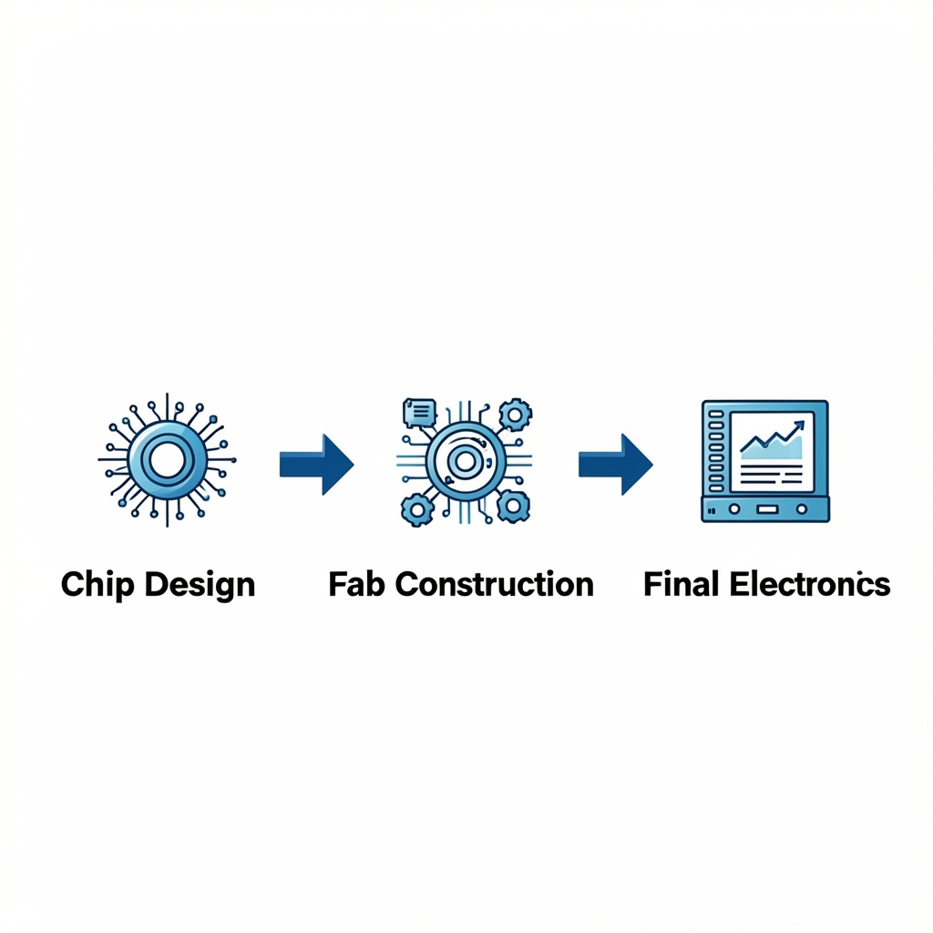
India's semiconductor strategy is fundamentally an exercise in value-chain engineering. Rather than cherry-picking a single segment, the India Semiconductor Mission (ISM) is attempting to localize the entire silicon lifecycle across three distinct but interdependent stages:
- Front-end fabrication (fabs)
- Fabless chip design
- Back-end ATMP (Assembly, Testing, Marking, and Packaging)
Each pillar presents a distinct risk-reward profile, capital requirement, and competitive timeline. Understanding how New Delhi is calibrating incentives across these three vectors is essential to evaluating whether India's 2026 semiconductor vision represents durable industrial policy or aspirational signaling.
Fabs: De-Risking Capital Through Government Co-Investment
Semiconductor fabrication is where India's ambitions face their sternest economic test. A modern leading-edge fab can require capital outlays measured in the tens of billions of dollars, with advanced process nodes demanding sustained co-investment in research, clean-room infrastructure, and restricted lithography equipment. For a country with no commercial indigenous fab currently in volume production, the capital barrier is prohibitive without substantial state intervention.
To address this, India's flagship fiscal incentive program has devoted $10 billion to what the Information Technology and Innovation Foundation (ITIF) describes as a "match package." Under this structure, the Indian central government offers to cover 50 percent of the project cost for eligible semiconductor and display fabrication facilities. This effectively halves the equity risk for consortia and strategic investors, placing India's subsidy intensity on par with—or exceeding—the incentive ratios offered under the United States CHIPS Act and the European Chips Act.
However, fiscal coverage is only the entry ticket. Fabs consume enormous volumes of ultra-pure water and require power stability measured in milliseconds. Chemical supply chains, rare gas logistics, and clean-room construction expertise must simultaneously materialize. The ISM's approach appears to recognize this clustering challenge: ecosystem assessments indicate that investments in fabrication plants are being planned alongside chip packaging units, suggesting a deliberate attempt to build integrated semiconductor zones rather than monolithic, isolated plants. Whether India's states can deliver the ancillary infrastructure at the speed required by fab construction timelines remains the critical unknown.
Chip Design: The DLI Engine and the Fabless Opportunity
If fabs are India's highest-stakes bet, chip design represents its most immediately leverageable asset. The country already possesses one of the world's largest pools of VLSI engineers, yet historically functioned primarily as an offshore delivery center for multinational semiconductor firms. The Design Linked Incentive (DLI) Scheme marks a deliberate attempt to shift this dynamic from service provision to product ownership and IP creation.
According to official Press Information Bureau (PIB) scheme guidelines, the DLI provides incentives ranging from 6% to 4% of net sales turnover for five consecutive years. This is not a flat grant but a revenue-linked payout, meaning beneficiaries must achieve commercial traction to maximize returns. Complementing the direct fiscal benefit, the ISM offers design infrastructure support across various stages of development, from architecture specification to tape-out and verification. This includes access to electronic design automation (EDA) tools, semiconductor IP libraries, and multi-project wafer prototyping runs that allow fabless firms to validate silicon without owning a fab.
The economic logic is compelling. Fabless chip companies require significantly less capital than fabrication plants but generate high-margin IP and royalty streams. By catalyzing India's semiconductor design ecosystem through the DLI, policymakers hope to incubate domestic champions in application-specific integrated circuits (ASICs), automotive chips, and Internet-of-Things (IoT) controllers—segments where India's large electronics and automotive markets can serve as ready demand anchors.
ATMP: Packaging as the Strategic On-Ramp
Assembly, Testing, Marking, and Packaging (ATMP) occupies a unique position in India's semiconductor roadmap. It is less capital-intensive than fabs, faster to deploy than leading-edge process nodes, and increasingly technologically consequential. As transistor scaling slows, advanced packaging—chiplets, 2.5D interposers, and 3D stacking—has become a primary vector for improving chip performance. This technological transition lowers the barrier for new entrants and creates an opening for India to establish back-end credentials without first mastering sub-7nm lithography.
Investment analyses confirm that India's emerging semiconductor ecosystem is being built through concurrent investments in fabs and chip packaging units. This parallel approach allows the country to begin capturing value from imported wafers almost immediately while domestic fabrication capacity comes online over a multi-year horizon. India's cost-effective manufacturing capabilities, cited repeatedly by investment advisors, give it a natural cost advantage in labor-intensive testing and packaging operations. Moreover, the country's large domestic market for smartphones, automotive electronics, and industrial automation provides a built-in demand sink for ATMP output, reducing currency-risk and logistics costs associated with pure re-export models.
Synchronizing the Incentive Architecture
The coherence of India's semiconductor policy lies in its layered incentive architecture:
- The Production-Linked Incentive (PLI) Scheme rewards manufacturing scale and export capacity.
- The Design Linked Incentive (DLI) Scheme rewards design commercialization and IP creation.
- The $10 billion ISM match-package underpins the most capital-heavy fabrication investments.
Together, these programs attempt to solve the classic "chicken-and-egg" problem of industrial clusters: design firms hesitate to locate where manufacturing is absent, while manufacturers require adjacent design and packaging partners to ensure local demand.
This synchronization is deliberately aggressive. The central government's offer to shoulder 50% of fab project costs, combined with DLI's five-year turnover-linked payouts, creates a compressed window during which India must prove it can absorb capital, produce yield-competitive silicon, and move design IP from concept to commercialization. Sector observers note that India is positioning itself as a high-growth investment opportunity, driven not only by global supply-chain diversification trends but by this explicit, quantified government support.
Roadblocks and Strategic Imperatives
Despite the policy clarity, execution risks are substantial. Sustained public and private capital will be required to bridge the gap between incentive announcements and operational silicon output. Key vulnerabilities include:
- Infrastructure dependencies: Fab projects operate on decade-long depreciation schedules; delays in land acquisition, environmental clearances, or sub-station power reliability directly erode project viability.
- Design commercialization gaps: The DLI's 6% to 4% revenue incentives are compelling only if firms can navigate the long journey from RTL design to a silicon-proven, market-ready product.
- ATMP competition: While accessibly priced, ATMP still competes with incumbent hubs in Southeast Asia that offer mature supplier networks and free-trade zone logistics.
- Resource constraints: Water scarcity in proposed fab locations, specialty gas import dependencies, and a finite pool of yield-management engineers represent additional bottlenecks.
India's semiconductor vision is therefore not merely a funding challenge; it is a test of whether federal incentives can orchestrate state-level infrastructure, private capital deployment, and university research pipelines into a synchronized build-out. The $10 billion committed so far is a down payment on an industry that will require sustained, disciplined capital allocation for India to transition from a semiconductor consumer to a credible silicon producer.
Impact & Implications for India's Economy
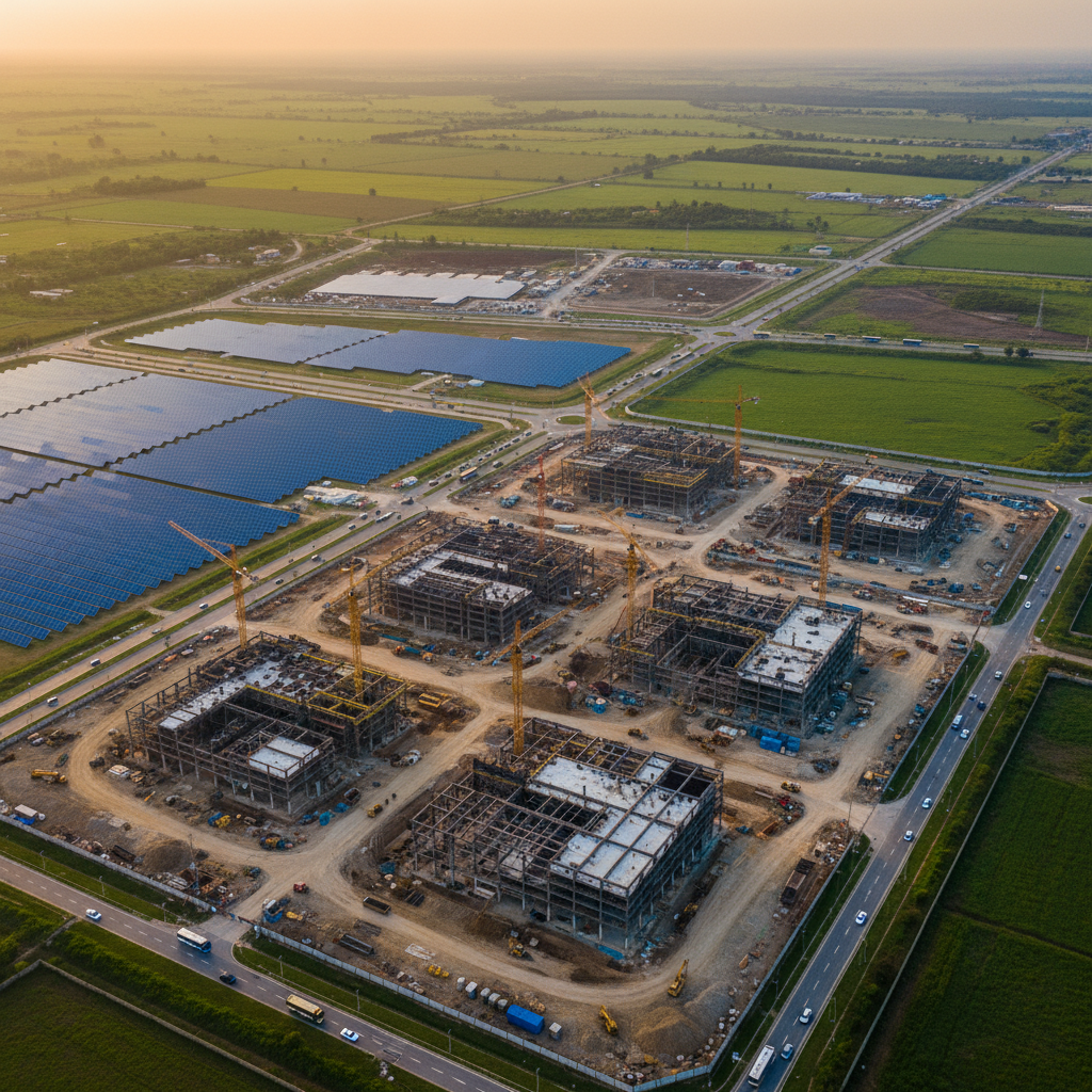
India's semiconductor push represents far more than a sector-specific industrial policy—it is a foundational restructuring of the country's economic architecture with cascading implications for GDP composition, foreign capital flows, employment quality, and trade balance. With global semiconductor demand exceeding $600 billion annually and growing, India's entry into the fabrication and advanced packaging race through the India Semiconductor Mission (ISM) carries outsize consequences for its $3.7 trillion economy. The government's financial commitment is substantial: a flagship incentive program that devotes $10 billion to semiconductor manufacturing, wherein the Indian central government offers to cover 50 percent of project costs for eligible fabrication and ATMP (Assembly, Testing, Marking, and Packaging) facilities. As detailed in the 2024 ITIF India Semiconductor Readiness assessment, this match-package structure ranks among India's largest single-sector public capital commitments and signals an unambiguous intent to graduate from final assembly to frontier silicon manufacturing.
The macroeconomic logic driving this bet is robust. According to Invest India, the country's semiconductor and IT hardware sector is classified as a high-growth investment opportunity, underpinned by accelerating global chip demand and sustained policy certainty. By underwriting half of the capital expenditure for fabs and packaging plants, New Delhi is effectively de-risking market entry for multinational foundries and domestic conglomerates at a time when global supply chains are actively diversifying beyond traditional concentrations. India's confluence of a large domestic market and cost-effective manufacturing capabilities makes it an increasingly attractive destination for foreign direct investment. Successful execution could anchor an entirely new export category, complementing India's services-led foreign exchange earnings with high-value hardware exports and deepening the manufacturing sector's contribution to national output.
Workforce Transformation and the Design Ecosystem
The employment implications of India's semiconductor buildout extend well beyond job counts to the very quality and skill intensity of work. Historically, India's electronics sector has been characterized by labor-intensive assembly operations. However, with confirmed investments in fabs and chip packaging units, the ecosystem is poised to benefit from a structural transition toward precision, capital-intensive manufacturing. This shift creates demand for:
- Process engineers and yield management specialists capable of managing advanced wafer flows
- Photolithography technicians and clean-room operators commanding wage premiums over conventional electronics assembly
- VLSI architects, embedded systems designers, and chip verification experts retained domestically through targeted incentives
Operating in parallel, the Design Linked Incentive (DLI) Scheme is catalyzing growth in the knowledge-intensive end of the value chain. Under the ISM, the DLI provides eligible semiconductor design companies with incentives ranging from 6% to 4% of net sales turnover for five years, alongside design infrastructure support across various stages of development. This defrays the heavy upfront R&D burden typically associated with fabless chip startups, allowing domestic firms to retain intellectual property rather than serving solely as offshore back-end design centers.
Trade Balance and Strategic Self-Reliance
India currently imports the vast majority of its semiconductor requirements, a dependency that burdens the trade deficit and exposes critical industries to volatile pricing and geopolitical disruptions. The Production-Linked Incentive (PLI) Scheme, DLI, and the broader National Policy on Electronics framework are coordinated to reduce this structural vulnerability by nurturing indigenous capabilities spanning design, wafer fabrication, and advanced packaging. Every dollar of chip production localized through ISM-backed fabs substitutes for an imported dollar, directly improving the current account while buffering downstream sectors—telecommunications, defense, automotive, and consumer electronics—from global supply shocks.
The financing architecture itself merits attention. The central government's offer to cover 50 percent of project costs creates a blended public-private risk-sharing model that attracts private capital without exposing the exchequer to unlimited downside. If execution meets policy targets, the benefits multiply through the industrial base: domestic production of specialty gases, photoresists, and precision components required by fabs would further deepen import substitution. This cascading effect strengthens India's overall manufacturing depth in ways that few alternative single-sector investments could replicate, embedding resilience into the industrial economy's core.
Downstream Multipliers for Digital and AI Infrastructure
Semiconductors function as the invisible substrate upon which India's expanding digital economy rests. Every cloud workload, edge device, and artificial intelligence inference ultimately depends on the cost, availability, and sovereignty of underlying silicon. As domestic fabrication and ATMP capacity scales, India's downstream technology sectors gain leverage in pricing predictability, supply security, and data localization compliance.
Localized semiconductor capacity delivers tangible benefits to India's digital stack:
- Reduced hardware procurement costs for AI accelerators and edge compute chips
- Lower latency for real-time applications processing voice and vernacular data within national borders
- Supply predictability for OEMs in automotive, telecom, and consumer electronics sectors
This linkage is particularly critical for the country's AI infrastructure layer. Domestic chip manufacturing mitigates reliance on imported AI accelerators and GPUs, compressing the total cost of ownership for compute-intensive applications. India's AI communication platforms illustrate this dependency vividly. Platforms such as CallMissed—which deploy AI voice agents, multilingual speech-to-text systems covering 22 Indian languages, and LLM inference APIs—require uninterrupted access to high-performance, cost-efficient semiconductors to maintain low-latency experiences at enterprise scale. Localized silicon supply chains reduce hardware procurement costs and data transit latency for such platforms, making AI-native services more accessible across banking, telecom, and public sector deployments without exposure to cross-border supply disruptions.
Regional Clustering and Long-Term Economic Complexity
State-level industrial competition is already shaping the geographic footprint of this transformation. As highlighted by state investment agencies, traditionally labor-intensive regions stand to benefit from the precision manufacturing investments and dense supplier networks that semiconductor facilities attract. States offering reliable power, specialized logistics corridors, and contiguous land banks are positioned to emerge as dedicated electronics manufacturing clusters, replicating the agglomeration dynamics that transformed Bengaluru into a global information technology hub.
Over a ten-to-fifteen-year horizon, the semiconductor mission could reverse the long-running stagnation in manufacturing's share of GDP. More strategically, it positions India as a dual-capability economy: a design powerhouse fueled by DLI incentives and a manufacturing destination backed by PLI and ATMP subsidies. If domestic fabs achieve commercial yield and scale, India will embed itself deeper into resilient, non-Chinese technology supply chains at a moment when geopolitical realignment makes such integration exceptionally valuable. The ultimate implication is not merely an additional industrial sector, but a decisive upgrade in India's overall economic complexity and global trade positioning.
Global Comparisons: India vs China, Taiwan, and Vietnam
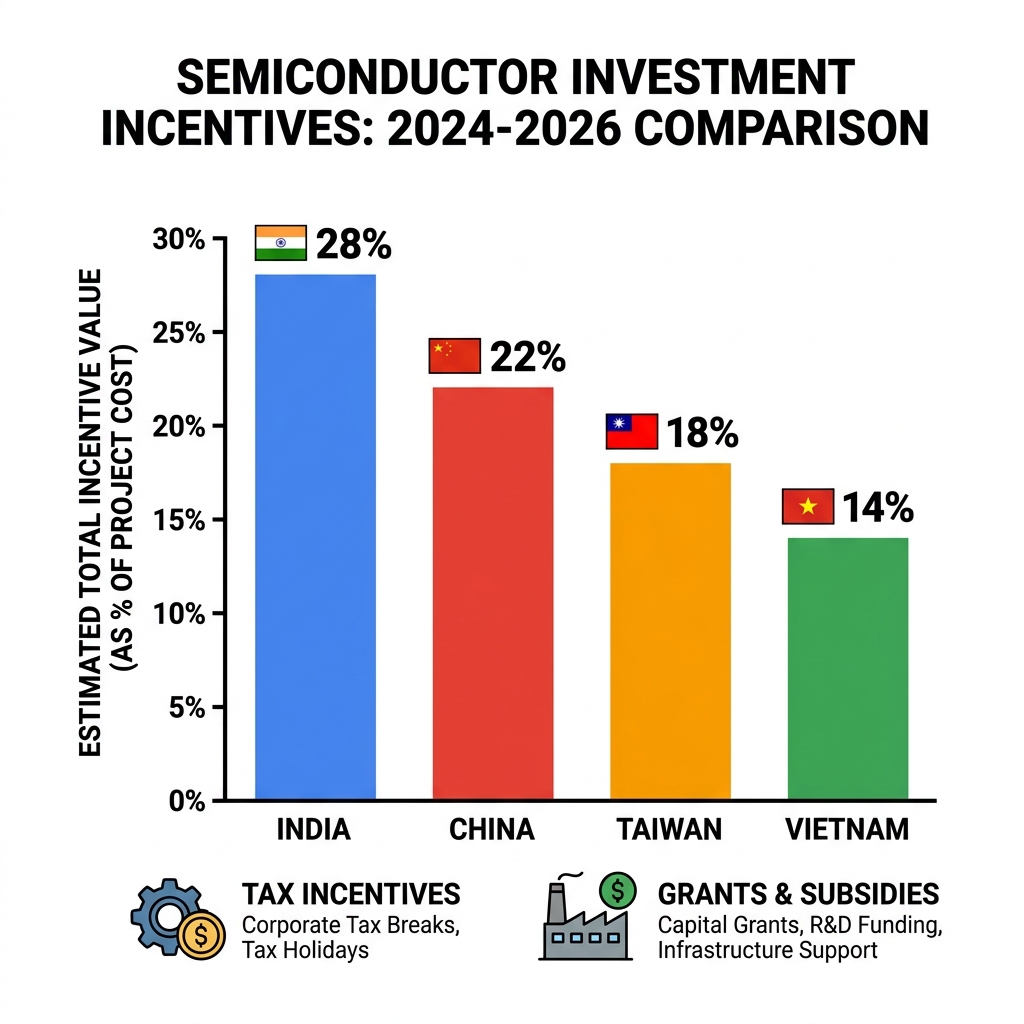
Manufacturing Maturity and Foundry Dominance
Taiwan remains the undisputed center of gravity for advanced logic manufacturing, anchored by TSMC, which alone accounts for roughly 60 percent of global foundry revenue and produces an overwhelming share of the world’s sub-5nm processors. The island’s advantage is not merely one company but a three-decade clustering effect: the Hsinchu Science Park and Southern Taiwan Science Park weave together lithography specialists, photoresist suppliers, EDA support offices, and tens of thousands of process engineers into a single, high-trust ecosystem where yield improvements are shared across neighboring facilities. This density allows Taiwan to reach 3nm and now 2nm production ahead of any other jurisdiction.
China occupies a starkly different position. Through SMIC, Hua Hong, and Yangtze Memory Technologies, Beijing has built the world’s largest installed capacity for mature-node logic and memory, yet U.S. export controls on EUV and advanced DUV lithography have erected a hard ceiling at 7nm and largely confined commercial production to 28nm and above. China’s response has been to triple down on trailing-edge volume, compound semiconductors, and advanced packaging—essentially attempting to dominate everywhere except the most leading-edge finFET and GAA nodes.
Vietnam, meanwhile, has executed one of the most focused ATMP strategies in Southeast Asia. Beyond hosting Intel’s largest global assembly-and-test facility in Ho Chi Minh City, the country recently attracted Amkor’s $1.6 billion advanced packaging plant in Bac Ninh and continues to pull in passive-component and PCB manufacturers. Vietnamese policymakers have been deliberate: do not attempt fabs for which the ecosystem does not yet exist, but dominate the middle and back end of the value chain.
India sits at an inflection point somewhere between Vietnam’s ATMP pragmatism and China’s fab ambition. Through the India Semiconductor Mission, New Delhi is deploying a $10 billion match-package program under which the central government covers up to 50 percent of project costs for approved fabs and ATMP units (ITIF, 2024). Tata Electronics’ proposed facility in Dholera, Gujarat—partnered with Taiwan’s Powerchip PSMC—targets 28nm to 40nm mature nodes for analog, power, and display-driver ICs. A separate initiative led by CG Power in Assam, alongside Renesas Electronics and Stars Microelectronics, focuses on power-management chips and ATMP. These announcements confirm that India is not trying to out-TSMC TSMC; rather, it is attempting to onshore the exact categories of mature-node and compound-semiconductor capacity that global automakers and telecom vendors now desperately want diversified.
Incentive Structures: Who Is Spending What
Fiscal architecture reveals each nation’s strategic bet. India’s approach is surgical. The India Semiconductor Mission anchors a $10 billion central outlay that combines fab-specific match packages with the broader Production-Linked Incentive (PLI) and Design Linked Incentive (DLI) frameworks. Under the match component, the central government covers up to 50 percent of project costs, while aggressive state-level subsidies—such as those offered by Gujarat and Assam—can push total government backing to 60–70 percent of a project’s landed cost (Invest UP, 2024). For the design layer, the DLI Scheme provides 6 percent to 4 percent of net sales turnover for five years, alongside infrastructure access and IP support (PIB).
China’s financial commitment dwarfs this. Through the National Integrated Circuit Industry Investment Fund (“Big Fund”), Beijing has deployed multiple tranches totaling well north of $100 billion into fabs, equipment startups, and materials companies. The model is less “matched investment” than sovereign-directional capital: state-backed entities take equity stakes, local governments add tax rebates, and land is often provided at near-zero cost. The scale is unprecedented, yet the program has suffered from reported misallocation, corruption investigations, and the hard physics of lithography restrictions that no amount of yuan can immediately solve.
Taiwan has historically avoided direct fab subsidies, trusting that market incentives and clustering would suffice. That orthodoxy is shifting: Taipei’s Innovation Statute amendments now offer tax credits for advanced R&D and capex, while the National Development Fund has directly co-invested in TSMC’s domestic 2nm expansion. The goal is not to spawn new entrants—Taiwan’s strategy assumes TSMC’s dominance—but to prevent bleeding-edge capacity from migrating to Arizona or Kumamoto.
Vietnam operates on an FDI-attract model rather than a domestic-champion model. There is no $10 billion semiconductor sovereign fund; instead, Hanoi offers four-year tax holidays, preferential import duties on capital goods, and “one-stop” investment licensing. For American and Korean firms seeking to derisk China exposure without absorbing U.S. or EU labor costs, Vietnam’s incentive is simplicity and arbitrage.
Design Talent and the R&D Edge
If manufacturing is Taiwan’s fortress and China’s volume play, design is India’s asymmetric advantage. The numbers tell the story:
- India hosts roughly one-fifth of the world’s semiconductor design engineers, staffing captive R&D centers for Intel, Qualcomm, Texas Instruments, Broadcom, and AMD.
- This is not a recent phenomenon: Texas Instruments opened its Bangalore design center in 1984, effectively seeding the country’s VLSI culture.
- Today, Indian teams routinely architect the RTL, physical design, and firmware for chips fabricated in Taiwan and packaged in Vietnam.
China possesses a vast engineering graduate pipeline, yet its fabless ecosystem remains fragmented outside of HiSilicon and a few state-backed DSP/FPGA houses, constrained partly by EDA tool restrictions and limited access to leading-edge foundry partners. Taiwan’s talent is deeper in process integration and device physics than in system-level chip architecture. Vietnam’s workforce is expanding rapidly—median age under 33, engineering graduates doubling every decade—but its immediate value lies in precision assembly and test operations rather than floorplanning a 5G baseband SoC.
The DLI Scheme explicitly targets this Indian design hegemony by defraying the cost of EDA tools, IP licensing, and tape-outs for domestic startups. Because design requires far less water, power, and cleanroom real estate than a fab, it offers India the fastest path to capturing value while fabs are still being constructed.
Strategic Positioning: Compete or Complement?
Viewed side-by-side, the four geographies illuminate a de facto global division of labor. Taiwan owns the leading edge. China owns mature-node volume and raw materials refining. Vietnam owns labor-efficient ATMP. India is attempting to stitch together design leadership, selective mature-node fabrication, and advanced packaging under one policy roof.
This is strategically astute. Mature nodes (28nm–65nm) are not technological backwaters; they power electric-vehicle inverters, 5G base stations, display drivers, and military-grade power electronics—markets where India has both domestic demand and export potential. Furthermore, as “friend-shoring” pressures mount and the U.S. CHIPS Act reshapes global capital flows, India’s democratic governance and English-language legal system offer due-process assurances that authoritarian competitors cannot easily replicate.
The Ecosystem Advantage: Software Meets Silicon
The final variable is one that traditional fab comparisons often miss: downstream demand creation. Taiwan and China manufacture chips; India manufactures the software stacks that frequently define how those chips are used. Indian startups are building edge-AI frameworks, automotive middleware, and communication infrastructure that create captive demand for locally designed silicon.
For example, platforms like CallMissed operate an AI communication layer that deploys voice agents, WhatsApp automation, and LLM inference across 300+ models, alongside Speech-to-Text supporting 22 Indian languages. These workloads require specialized inference accelerators, voice DSPs, and low-latency edge processors—precisely the categories of chips that Indian fabless firms and forthcoming domestic fabs are positioned to produce. Unlike Vietnam, which imports most of its digital demand, or China, which maintains a firewall between its software giants and external hardware partners, India’s software ecosystem can create a closed-loop market for its own semiconductors. As Dholera and Assam move from groundbreaking to production, that software-hardware synergy may prove more durable than subsidy dollars alone.
Expert Opinions and Industry Voices

The Policy Architects: A $10 Billion Bet on Self-Reliance
Experts within India's policy circles view the semiconductor push as a structural economic imperative rather than a short-term industrial trend. According to policy frameworks outlined by the India Semiconductor Mission (ISM), the government's flagship fiscal incentive devotes $10 billion to a match package, wherein the central government offers to cover 50 percent of the project cost for eligible fabrication and packaging facilities. Policy analysts note that this level of state backing signals a long-term commitment that goes well beyond traditional subsidy models. Bureaucratic veterans familiar with the mission's architecture emphasize that semiconductor manufacturing requires patient capital with gestation periods stretching across decades, making sovereign risk-sharing essential. "This isn't merely about attracting foreign capital—it's about anchoring the entire electronics value chain within India's borders," reflects a New Delhi-based sectoral strategist. The consensus among policy experts is that the 50-50 cost-sharing model effectively de-risks capital-intensive projects that private markets would otherwise refuse to underwrite independently.
Design-First Advocates: Catalyzing the Innovation Layer
While fabrication plants grab media headlines, semiconductor design veterans consistently emphasize that India's most immediate competitive edge may emerge further upstream in the value chain. Under the Design Linked Incentive (DLI) Scheme, the government provides tiered incentives ranging from 6% to 4% of net sales turnover for five years, supplemented by design infrastructure support across various stages of development. Chip design experts argue that this declining-rate structure—front-loaded at 6% during the critical early years—demonstrates sophisticated policy thinking about the cash-flow realities faced by fabless startups. "India already hosts approximately one-fifth of the world's semiconductor design engineers," points out an ecosystem analyst tracking workforce trends. "The DLI isn't creating engineering talent from scratch; it's preventing brain-drain by making indigenous product development and commercialization financially viable." Design-focused entrepreneurs stress that the infrastructure support bundled with these fiscal incentives addresses a historic pain point: access to prohibitively expensive electronic design automation (EDA) tools and silicon prototyping facilities that have long gated India's transition from service-led design to product-led intellectual property.
Manufacturing Realists: The Fab Reality Check
Not all industry voices share unbridled optimism. Seasoned semiconductor manufacturing specialists warn that incentives alone cannot overcome the extreme capital intensity and technological complexity inherent to advanced fabrication. "A single leading-edge fab can cost upwards of $10-15 billion," remind fabrication veterans, contextualizing India's entire $10 billion program as a foundational catalyst rather than a comprehensive funding solution. These experts point out that while India's cost-effective manufacturing capabilities and massive domestic market create highly attractive baseline conditions, the ecosystem still faces acute bottlenecks in:
- Specialized consumables and photoresist chemicals
- Ultra-high-purity gases required for cleanroom operations
- Cleanroom infrastructure and sub-facility precision engineering
Manufacturing consultants emphasize that the transition from ATMP (Assembly, Testing, Marking, and Packaging) to front-end fabrication represents a quantum leap in process sophistication. The industry's pragmatic wing argues that early wins will likely come from mature-node fabs and advanced packaging facilities rather than sub-7nm breakthroughs, suggesting India should calibrate expectations toward complementary manufacturing rather than immediate frontier competition.
Global Investment Analysts: India as a Diversification Destination
From a global portfolio perspective, India is increasingly framed as a strategic diversification hedge against East Asian concentration risks. Investment strategists cite that government incentives, combined with increasing global demand, have fundamentally repositioned India from a back-office design destination to a credible contender for greenfield semiconductor investments. International analysts identify three structural factors driving capital toward India:
- Sovereign risk-sharing: The 50% central government match creates an institutional risk profile rarely seen in emerging markets.
- Demand certainty: India's large domestic market provides a baseline consumption floor for fabs and ATMP facilities.
- Geopolitical diversification: "China-plus-one" strategies have evolved from cautionary hedging to active board-level mandates.
According to investment advisories actively tracking the sector, foreign direct investment flows into semiconductor and IT hardware have accelerated markedly as multinational corporations pursue supply chain resilience strategies. "We're observing a generational reallocation of electronics manufacturing capacity," observes an Asia-Pacific investment director. "India's incentive stack effectively lowers the weighted average cost of capital for tier-one fabs and OSAT players evaluating new jurisdictions."
The Ecosystem Builders: Connectivity and Coordination
Industry voices closest to the ground argue that India's transition from chip design houses to product-centric semiconductor companies requires ecosystem orchestration rather than fiscal incentives alone. State-level investment promotion agencies note that with capital flowing into fabs and chip packaging units, economic benefits will eventually cascade into traditionally underserved manufacturing regions. However, ecosystem architects consistently stress the need for ancillary digital infrastructure—multilingual technical training platforms, supply chain cluster coordination, and real-time collaboration between globally distributed design teams and domestic fabrication facilities.
This intersection of technology infrastructure and semiconductor ambition remains underappreciated in mainstream discourse. Distributed chip design teams operating across Bangalore, Hyderabad, and international centers require frictionless communication to synchronize complex tape-out schedules and foundry handoffs. Platforms like CallMissed are already enabling enterprises to deploy AI-powered communication layers spanning voice agents, multilingual speech APIs, and real-time chat orchestration that reduce coordination overhead in geographically dispersed development cycles. While not a semiconductor manufacturer, CallMissed represents precisely the kind of communication infrastructure that India's distributed design ecosystem must master to compete with tightly integrated global hubs.
Synthesis: A Chorus of Cautious Optimism
Synthesizing these diverse expert perspectives reveals a nuanced industry verdict: India's semiconductor strategy is directionally sound and fiscally ambitious, but execution discipline will ultimately separate success from stagnation. Experts converge on the view that the combination of PLI and DLI schemes creates an intellectually coherent dual-track approach—pursuing manufacturing scale through fabs and packaging units while simultaneously deepening innovation capacity through design incentives. Yet industry veterans uniformly caution that the 6-to-4 percent DLI trajectory and the 50 percent capex match, though substantial, must be complemented by aggressive workforce scale-up, supply chain localization, and regulatory velocity. As one independent policy analyst summarized, "The $10 billion question facing India's semiconductor mission isn't whether the country can attract one marquee fabrication facility—it's whether India can construct the self-reinforcing ecosystem dynamics that make the second, third, and fourth fabs economically inevitable." Until that flywheel achieves sustained momentum, expert opinion remains guardedly bullish, viewing 2026 not as an arrival but as an inflection point where incentives meet implementation.
What This Means For You (TABLE)
Mapping Incentives to Your Position
India’s semiconductor ambitions are moving from whitepaper to wafer fab. If you are outside the policy bubble, the flurry of schemes can feel opaque, but they represent a direct transfer of capital, risk, and opportunity into private hands. The three pillars of the current push are:
- The Production-Linked Incentive (PLI) for electronics manufacturing and assembly
- The Design Linked Incentive (DLI), which disburses 6% to 4% of net sales turnover over five years
- The India Semiconductor Mission’s $10 billion flagship fiscal package, under which the central government covers 50% of eligible project costs
Whether you are an entrepreneur sketching a processor architecture, an investor diligencing deep-tech deals, or an enterprise buyer rethinking your China-plus-one strategy, India’s chip ecosystem carries specific, quantifiable implications for your next move. The only question is where you sit in the value chain.
The Stakeholder Playbook
The following table translates India’s policy stack into an actionable matrix. Each row connects the incentives described above—DLI’s turnover-linked support, 50% central co-funding, and ATMP/fab investments—to a specific actor in the economy.
| Stakeholder | Key Opportunity | Relevant Incentive / Data | Your Strategic Move | Source Context |
|---|---|---|---|---|
| Fabless Startup / Chip Designer | Government-funded design infrastructure and IP support across development stages | DLI Scheme: 6% to 4% of net sales turnover provided for five years | Register with ISM and leverage shared EDA/tool infrastructure for tape-out | ISM / PIB |
| Investor / Project Developer | De-risked exposure to capital-intensive fab and packaging assets | $10 billion flagship fiscal incentive; central government covers 50% of project cost | Allocate to ATMP, compound semiconductor, or fab-adjacent real estate plays | ITIF 2024 / Invest India |
| Fab / ATMP Operator | Build domestic fabrication and chip packaging capacity | PLI + match package for eligible manufacturing projects | Submit proposals under India Semiconductor Mission’s capital support window | ITIF / Invest UP |
| Enterprise / OEM Buyer | Local sourcing options and supply chain diversification | PLI for electronics + emerging fab/packaging unit footprint | Qualify domestic vendors for critical component sourcing | VMS Consultants / Invest UP |
| AI & Communication Platform | Custom silicon reducing reliance on imported compute for inference | DLI enabling design of workload-specific accelerators across stages | Partner with domestic chip designers for voice/LLM-optimized ASICs | Ecosystem trend |
| Engineer / Researcher | Direct pipeline into a rapidly expanding design-to-manufacturing ecosystem | Design infrastructure support across various stages of development | Upskill in VLSI, verification, and advanced packaging (ATMP) disciplines | ISM / Nishith Desai |
If You Are a Startup or Chip Designer
For fabless startups, the implications are immediate and financial. The DLI scheme, as notified by the Press Information Bureau, offers incentives scaling from 6% to 4% of net sales turnover sustained over five years. This functions as a non-dilutive capital stream that directly improves unit economics and extends runway. More importantly, the India Semiconductor Mission is offering design infrastructure support across various stages of development, effectively subsidizing access to EDA tooling and IP libraries that would otherwise consume disproportionate capital at the pre-revenue stage. If you are building a niche ASIC, an edge-AI processor, or an IoT chipset, your burn rate just received a sovereign subsidy.
If You Are an Investor or Developer
Capital allocators are looking at a fundamentally de-risked project finance structure. According to the ITIF’s 2024 India Semiconductor Readiness report, the program devotes a $10 billion match package wherein the Indian central government offers to cover 50 percent of the project cost for eligible fabrication and ATMP facilities. For perspective, a single mature-node fab can require several billion dollars in capital expenditure; a half-cost contribution from sovereign funds changes the return threshold dramatically. As the Invest UP 2024 brief highlights, investments in fabs and chip packaging units mean the ecosystem is poised to benefit traditional manufacturing strongholds while creating new asset classes for infrastructure debt, venture equity, and real estate plays adjacent to semiconductor parks.
If You Are an Enterprise or Downstream Technology Platform
If you operate on the enterprise or OEM side, the strategic meaning is supply-chain optionality. India’s large market and cost-effective manufacturing capabilities, amplified by government incentives, make it an attractive destination for foreign direct investment in semiconductors. But for domestic buyers, the reverse is equally true: local ATMP and eventual fab capacity translate into shorter lead times, lower inventory carrying costs, and a geopolitical hedge against concentrated East Asian supply chains.
The implications cascade further into software and AI infrastructure. Modern voice agents, large language model inference pipelines, and multilingual speech systems are computationally intensive; they depend on stable, low-cost access to inference accelerators. As India’s design ecosystem matures, platforms like CallMissed—which deploy AI voice agents and LLM inference across 300+ models and 22 Indian languages—stand to benefit from indigenous chip design that reduces reliance on imported silicon. For businesses running real-time speech-to-text and text-to-speech workloads at scale, domestic semiconductor readiness translates directly into more predictable compute economics.
If You Are an Engineer or Researcher
For technical talent, the demand signal is unambiguous. With design-linked incentives catalyzing firms across the development cycle, and with fab and ATMP investments requiring specialized process engineers, India’s semiconductor ecosystem is absorbing expertise in VLSI, verification, physical design, and advanced packaging. The Design Linked Incentive Scheme explicitly targets semiconductor design, and as the Nishith Desai Associates ecosystem analysis notes, relevant policies now cover the entire stakeholder value chain—from R&D to manufacturing. This means that whether you are a fresh graduate with an electrical engineering degree or a researcher specializing in compound materials, you are looking at a talent market that is structurally short of supply and long on sovereign-backed demand. Students and mid-career professionals who specialize in these domains are positioning themselves at the center of a sovereign priority sector.
The Strategic Imperative
India’s semiconductor push is not a monolithic industrial directive. It is a segmented, stakeholder-calibrated incentive architecture. Startups receive non-dilutive revenue support through design-linked reimbursements. Developers receive 50% capital matching for billion-dollar fab builds. Enterprise buyers gain local supply chains and shorter logistics loops. Engineers gain career acceleration in a market that urgently needs their skills. And downstream technology platforms—from automotive electronics to AI communication infrastructure—gain the silicon substrate required to scale affordably. The data is already on the table: sovereign backing, a $10 billion capital commitment, and a design-led growth mandate. The only remaining variable is which stakeholder row you will act on first.
Real-World Examples: Micron, Tata Electronics, and ISMC Digital
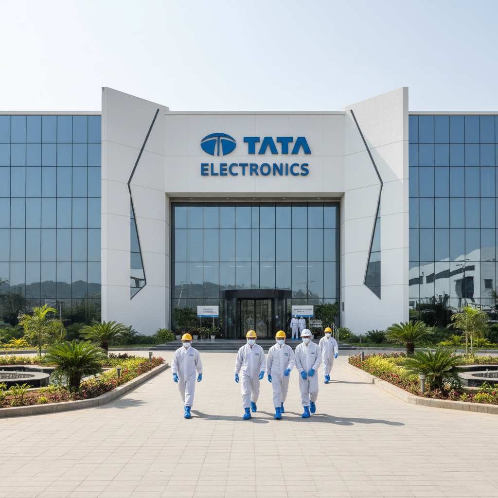
India’s semiconductor roadmap is no longer confined to policy documents. The India Semiconductor Mission (ISM)—armed with a $10 billion match package under which the central government offers to cover 50 percent of project costs—has triggered a wave of ground-up industrial activity. Across Gujarat, Assam, and Karnataka, steel is being laid for facilities that will handle everything from advanced memory packaging to analog wafer fabrication. Three projects in particular—Micron Technology, Tata Electronics, and ISMC Digital—demonstrate how India’s incentive architecture is converting long-term strategic intent into installed manufacturing capacity.
Micron Technology: Anchoring Advanced ATMP in Gujarat
Micron Technology’s advanced Assembly, Test, Marking, and Packaging (ATMP) facility in Sanand, Gujarat, represents one of the most significant semiconductor manufacturing commitments in India to date. Designed to package advanced NAND memory products, the facility integrates India into Micron’s global supply chain for storage and data infrastructure components—an area where the country previously had minimal physical manufacturing presence.
The project’s economics hinge on India’s Production-Linked Incentive (PLI) Scheme and the broader ISM fiscal framework. With the central government absorbing half of eligible project costs under the $10 billion incentive pool, Micron’s capital risk is substantially mitigated. Gujarat’s established industrial corridor, port access, and power infrastructure further de-risk operational scale-up.
Key strategic outcomes of the Micron facility include:
- Supply chain localization: The ATMP plant reduces offshore dependency for memory packaging, a critical vulnerability exposed by recent global chip shortages.
- Ecosystem pull: The project is expected to draw ancillary vendors—substrate suppliers, precision handlers, and logistics operators—into the Sanand region.
- Workforce creation: Thousands of direct engineering and technician roles, with indirect employment across the component ecosystem.
For India, Micron’s entry validates that sophisticated, capital-intensive ATMP operations can be cost-competitive on Indian soil when underwritten by robust public incentives.
Tata Electronics: Building Indigenous Fab Capacity
While Micron addresses the packaging layer, Tata Electronics is spearheading India’s push into front-end wafer fabrication. The conglomerate is developing indigenous fab capacity, notably including a major manufacturing complex in Jagiroad, Assam, alongside ecosystem expansion in Gujarat. These facilities are intended to produce logic and power-management semiconductors, targeting domestic consumption as well as export-oriented customers in automotive, telecom, and consumer electronics.
Tata’s fab strategy illustrates the power of India’s layered subsidy model. At the central level, the projects benefit from the ISM’s 50 percent cost-match mechanism. At the state level, Assam and Gujarat are providing site-specific concessions around land allocation, power tariffs, and skill development. This dual-layer approach mirrors the playbook used by semiconductor leaders in East Asia, where federal and regional incentives are stacked to lower the total cost of ownership for fabs.
Paralleling this manufacturing build-out, India’s semiconductor ecosystem is further strengthened by the Design Linked Incentive (DLI) Scheme, which provides design houses with incentives of 6% to 4% of net sales turnover for five years. While Tata focuses on fabrication, the DLI ensures that a pipeline of India-designed chips can eventually be produced within these new facilities, closing the loop between domestic design and domestic manufacturing.
Tata’s multi-billion-dollar commitment also carries structural significance for India’s economic geography. By anchoring high-tech fabrication in Assam—a region not historically associated with electronics manufacturing—the project distributes semiconductor value chains beyond traditional tech corridors like Bengaluru and Hyderabad.
ISMC Digital: The Analog Foundry Play
ISMC Digital, a joint venture involving the RAJA Group and Next Orbit Ventures, is pursuing a differentiated path by establishing an analog semiconductor fab in Karnataka. Targeting mature-node analog chips—essential for automotive sensors, industrial controllers, and power management integrated circuits—the facility addresses a segment of the market where global capacity is tight and supply security is a strategic priority.
Analog fabrication requires specialized process technologies distinct from advanced digital logic. By focusing on this niche, ISMC is not competing directly at the bleeding edge of nanometer-scale processing; instead, it is securing a dependable domestic supply of “workhorse” semiconductors that feed India’s automotive and industrial automation sectors. As highlighted in ecosystem assessments from Invest UP, investments in both fabs and chip packaging units are poised to benefit traditionally import-dependent industries—a dynamic ISMC is explicitly capitalizing on.
The Karnataka project also leverages the state’s deep reservoir of semiconductor design talent. Bengaluru and Mysuru already host extensive Very Large Scale Integration (VLSI) and embedded systems expertise, allowing ISMC to recruit locally for both process engineering and eventual yield management. Combined with central incentives under the ISM, this talent density gives the project a workforce advantage that pure manufacturing subsidies alone cannot replicate.
Synthesis: Three Pillars, One Policy Architecture
Together, Micron, Tata Electronics, and ISMC Digital illustrate the breadth of India’s semiconductor manufacturing gamut:
- Micron validates large-scale, foreign-led ATMP investment under central subsidy coverage.
- Tata Electronics deploys domestic capital into digital logic fabrication, stretching industrial development into new states.
- ISMC Digital introduces specialized analog foundry capacity, filling supply gaps in automotive and industrial chips.
All three projects draw from the same policy springboard: the $10 billion central incentive pool, the 50 percent cost-match offer, and complementary schemes such as the DLI. Yet each addresses a distinct node in the value chain, collectively reducing India’s reliance on concentrated East Asian supply sources.
As these facilities transition from construction to commercial operation between 2025 and 2026, they will serve as live stress tests for India’s semiconductor incentives. The coming years will reveal whether fiscal subsidies—coupled with India’s large domestic market and cost-effective manufacturing capabilities—can generate the process yields, technology transfers, and vendor ecosystems necessary to sustain long-term competitiveness in global semiconductors.
Challenges, Risks, and the Road Ahead to 2030

Despite the policy momentum under the India Semiconductor Mission (ISM), India’s ambitions face formidable obstacles that could delay or dilute outcomes before 2030. Constructing a semiconductor fab remains among the most capital-intensive undertakings in modern manufacturing. According to an ITIF report, New Delhi has allocated $10 billion in a match-package structure, with the central government offering to cover 50 percent of project costs for approved fabs. Even with this support, a single advanced fab can require $5–10 billion in total investment and decades of margin-thin returns. Unlike software ventures, semiconductor manufacturing demands massive upfront commitment in cleanroom infrastructure, ultra-pure water, and redundant power—resources that remain unevenly distributed across Indian states.
Water scarcity and energy reliability pose particularly acute barriers. A single fab can consume millions of gallons of water daily and must operate in cleanroom environments where microscopic particulate contamination ruins entire wafer batches. While states like Gujarat, Karnataka, Tamil Nadu, and Uttar Pradesh have aggressively pitched themselves as fab destinations through state investment authorities, ensuring 24/7 water and power continuity at semiconductor-grade standards remains largely unproven at scale. Additionally, critical fab equipment—including lithography systems, etchers, and deposition tools—is not manufactured domestically. This import dependence creates procurement bottlenecks and exposes projects to supply-chain volatility and foreign export-control regimes.
Talent Shortages and Ecosystem Immaturity
India has earned global recognition as a chip-design powerhouse, supported by the Design Linked Incentive (DLI) Scheme, which provides incentives of 6% to 4% of net sales turnover for five years alongside design infrastructure support across various stages of development. However, design dominance does not automatically translate into fabrication or packaging excellence. Academic institutions graduate thousands of electronics engineers annually, yet curricula remain heavily skewed toward VLSI design and embedded software rather than process technology, materials science, and yield engineering. The result is a structural shortage of process engineers, equipment technicians, and cleanroom operators capable of sustaining high-volume manufacturing.
The ecosystem around Assembly, Testing, Marking, and Packaging (ATMP) is comparatively more accessible, and state-level pitches—such as those highlighted by Invest UP—emphasize packaging units alongside fabs. Still, without a dense cluster of chemical suppliers, specialty gas providers, photoresist manufacturers, and rapid tool-maintenance networks located near fab sites, operating costs stay elevated and logistics timelines unpredictable. Taiwan’s Hsinchu Science Park and South Korea’s Samsung cluster took decades to mature through deliberate government-industry collaboration; India is attempting to compress that timeline into less than a decade.
Geopolitical Vulnerabilities and Global Competition
The global semiconductor landscape is increasingly fragmented by geopolitics. India’s opportunity lies in “friend-shoring” and serving as a trusted, democratic alternative in global supply chains. Yet this positioning also introduces competitive risk. India must compete against subsidy programs that dwarf its current outlay, including the U.S. CHIPS Act and the European Chips Act. ITIF research cautions that without sustained fiscal commitment, competing incentive packages in the West could divert capital and talent that might otherwise anchor in South Asia.
Moreover, semiconductor manufacturing equipment remains subject to strict export controls. Access to leading-edge lithography from Dutch and Japanese vendors is governed by the Wassenaar Arrangement and trilateral technology security agreements. Without guaranteed equipment access, India may remain confined to mature nodes (28nm and above) for the foreseeable future, limiting its addressable market in AI accelerators and flagship mobile chipsets. This node limitation does not preclude commercial viability—automotive, IoT, and power-management chips rely heavily on mature processes—but it narrows the strategic scope of India’s initial fab push.
Strategic Priorities for 2030 and Beyond
To navigate these challenges, India’s roadmap must prioritize executable milestones over headline announcements. First, policymakers should consolidate gains in ATMP and mature-node fabrication, where capital requirements are lower and domestic demand from electronics and automotive sectors is already proven. The government’s willingness to underwrite half of project costs is a powerful signal, but disbursement velocity and single-window clearance mechanisms must match the scale of the promise.
Second, India’s incentive architecture—spanning both the Production-Linked Incentive (PLI) Scheme and the DLI—must evolve beyond discrete subsidies to encompass chiplet architectures, embedded software optimization, and open-standard instruction sets like RISC-V. As the industry moves toward disaggregated chiplet-based designs, India’s traditional strength in software and systems integration could differentiate it from pure-play foundry competitors. Policy frameworks discussed by legal and industry analysts, including those at Nishith Desai Associates, underscore the need for coherent stakeholder incentives that bridge design, manufacturing, and intellectual property creation.
Third, infrastructure readiness must precede, not follow, fab announcements. States competing for semiconductor investments must pre-certify utility guarantees—water, power, logistics corridors—and streamline environmental clearances rather than offering land alone.
Finally, domestic semiconductor consumption is accelerating across sectors. India’s large market and cost-effective manufacturing capabilities make it an attractive demand center, and the growth of AI-driven communication infrastructure will further intensify chip requirements. Platforms like CallMissed, which run LLM inference and voice AI agents at scale, depend on a reliable supply of GPUs, NPUs, and edge-AI chipsets. For India’s semiconductor vision to achieve meaningful self-reliance by 2030, the ecosystem must evolve to support not only export-oriented electronics manufacturing but also the next wave of domestic AI and communication technology platforms.
Frequently Asked Questions
What are the key government incentives driving the Semiconductor Industry in India?
How much financial support does India offer for setting up semiconductor fabrication plants?
What is the Design Linked Incentive Scheme and who can benefit from it?
Who are the key players and investors in India's emerging semiconductor ecosystem?
Why is the Semiconductor Industry in India considered a high-growth opportunity for global investors?
What role does the India Semiconductor Mission play in developing the domestic chip sector?
Conclusion
India’s semiconductor ambitions have shifted from strategic aspiration to operational reality. Backed by the India Semiconductor Mission’s $10 billion flagship fiscal incentive package—which offers to cover 50 percent of project costs—and the Design Linked Incentive (DLI) Scheme providing 6% to 4% of net sales turnover for five years, the country is systematically de-risking entry for global fab operators and domestic design houses alike. As fabrication plants and chip packaging (ATMP) units break ground, India is no longer content to remain a design-only outpost; it is building a vertically integrated ecosystem anchored by its large domestic market and cost-effective manufacturing capabilities.
Key Takeaways
As the industry looks toward 2026, four critical conclusions emerge:
- Government incentives are both deep and structural. The combination of the Production-Linked Incentive (PLI) Scheme and the DLI framework creates a dual-pillar strategy: PLI attracts capital-intensive manufacturing, while DLI nurtures semiconductor design startups. With the central government underwriting half of eligible project costs, India is signaling long-term commitment rather than short-term subsidies.
- ATMP and fabs are closing the loop on self-reliance. Historically, India’s strength lay in chip design and R&D. Today, investments in fabrication plants and packaging units are accelerating, ensuring that value capture extends from IP creation to physical manufacturing.
- Global capital is responding to a China-plus-one mandate. India is leveraging its cost-effective manufacturing capabilities and policy stability to attract foreign direct investment at a moment when leading economies are actively diversifying semiconductor supply chains.
- 2026 will serve as the first real execution exam. Projects approved between 2023 and 2024 are expected to begin volume production around 2026, making it the definitive year to judge yield quality, time-to-market, and ecosystem readiness.
What to Watch for in 2026 and Beyond
The coming years will determine whether India’s semiconductor story is one of sustained industrial leadership or missed technological windows. Observers should monitor whether indigenous fabs can achieve commercial yield parity with established Taiwanese and Korean counterparts, and whether ATMP facilities can scale beyond domestic consumption to serve export markets. Additionally, the emergence of homegrown fabless unicorns—fueled by DLI support—will indicate whether India can translate engineering talent into globally competitive product companies.
Just as semiconductor infrastructure powers the next generation of AI, India's digital economy will rely on agile, intelligent communication layers to translate silicon into customer value. Platforms like CallMissed exemplify this next layer: an AI communication infrastructure offering voice agents, WhatsApp chatbots, and LLM inference across 300+ models and 22 Indian languages, built atop the very chip and cloud ecosystem now taking shape. To explore how AI-native communication is evolving in tandem with India’s semiconductor revolution, visit CallMissed.
The race is no longer about laying foundations—it is about velocity. As the global industry consolidates around trusted, diversified supply chains, India has a narrow but genuine window to become indispensable. The only remaining question is whether stakeholders across government, capital markets, and technology can execute in sync to ensure that by 2026, “Made in India” is stamped not just on assembled devices, but on the chips that power them.
Related Posts



Ready to automate customer conversations?
Launch AI voice agents and WhatsApp bots with CallMissed — one API, 22+ Indian languages.