India’s Semiconductor Revolution: Odisha’s MoU with Intel & 3DGS Ignites Chipmaking Ambitions
Did you know that India's semiconductor market is projected to reach $110 billion by 2030—yet the nation currently imports nearly all its advanced chips?...
India’s Semiconductor Revolution: Odisha’s MoU with Intel & 3DGS Ignites Chipmaking Ambitions
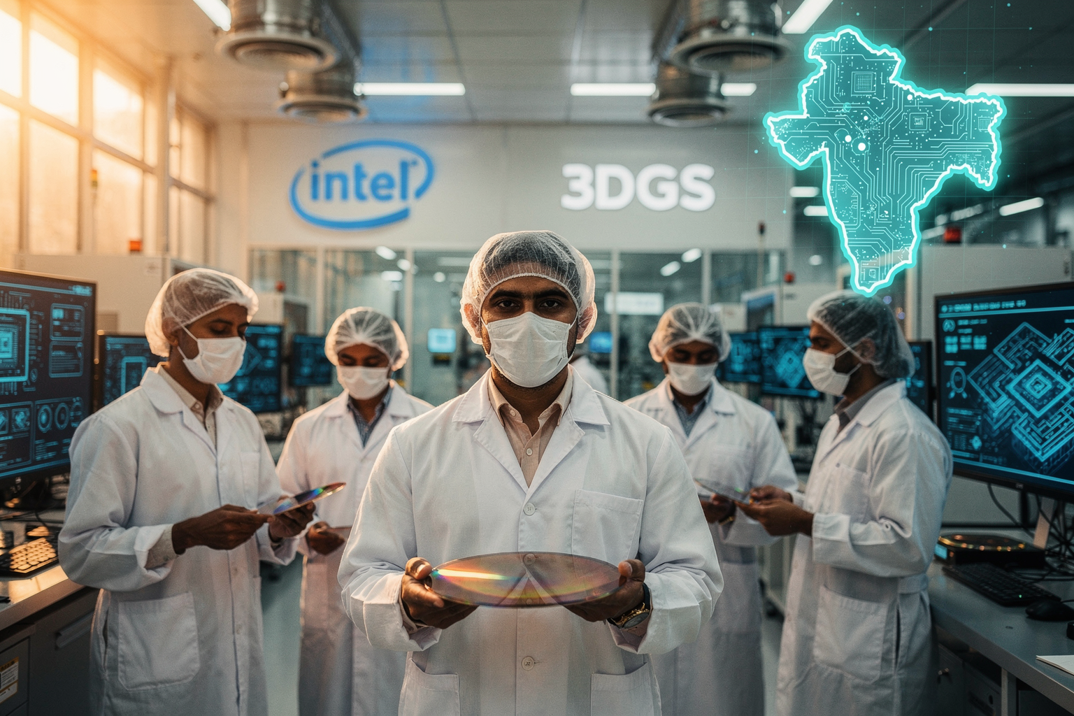
Did you know that India's semiconductor market is projected to reach $110 billion by 2030—yet the nation currently imports nearly all its advanced chips? This staggering gap between domestic consumption and local manufacturing explains why a state-level pact can create nationwide ripples. In May 2026, Odisha took center stage in India’s semiconductor revolution by signing a landmark Memorandum of Understanding (MoU) with global silicon giant Intel and advanced packaging pioneer 3D Glass Solutions (3DGS). This ambitious partnership, valued at $3.3 billion, isn’t just about building a new plant—it’s about bringing cutting-edge substrate manufacturing technology to Indian soil for the very first time.
Why is this move generating such excitement across tech and business circles? For starters, semiconductors underpin nearly every modern device—from smartphones to satellites—but India’s share in the global supply chain has historically been negligible. According to the Indian government, demand for electronics is expanding at 15% annually, and supply chain disruptions in recent years have driven home the risks of over-reliance on imports. With global chip shortages fresh in memory, India’s push for chipmaking self-sufficiency has never felt more urgent.
This blog unpacks the details behind Odisha’s game-changing partnership with Intel and 3DGS: what substrate technology means, how this project could redefine India’s manufacturing ecosystem, and why the global semiconductor industry is paying close attention. We’ll connect policy moves with real-world outcomes—from job creation and supply chain resilience to the latest opportunities for startups. Platforms like CallMissed, which leverage domestic chipmaking and AI infrastructure, showcase how a vibrant local semiconductor ecosystem can supercharge innovation across sectors.
Read on to discover how a single MoU could ignite India’s chipmaking ambitions and accelerate the country’s status as a global technology powerhouse.
Introduction
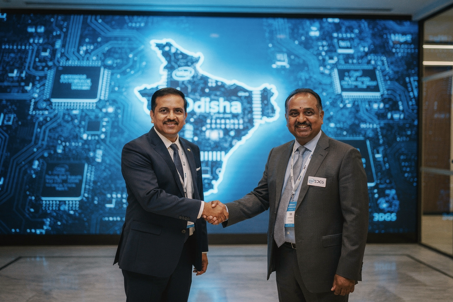
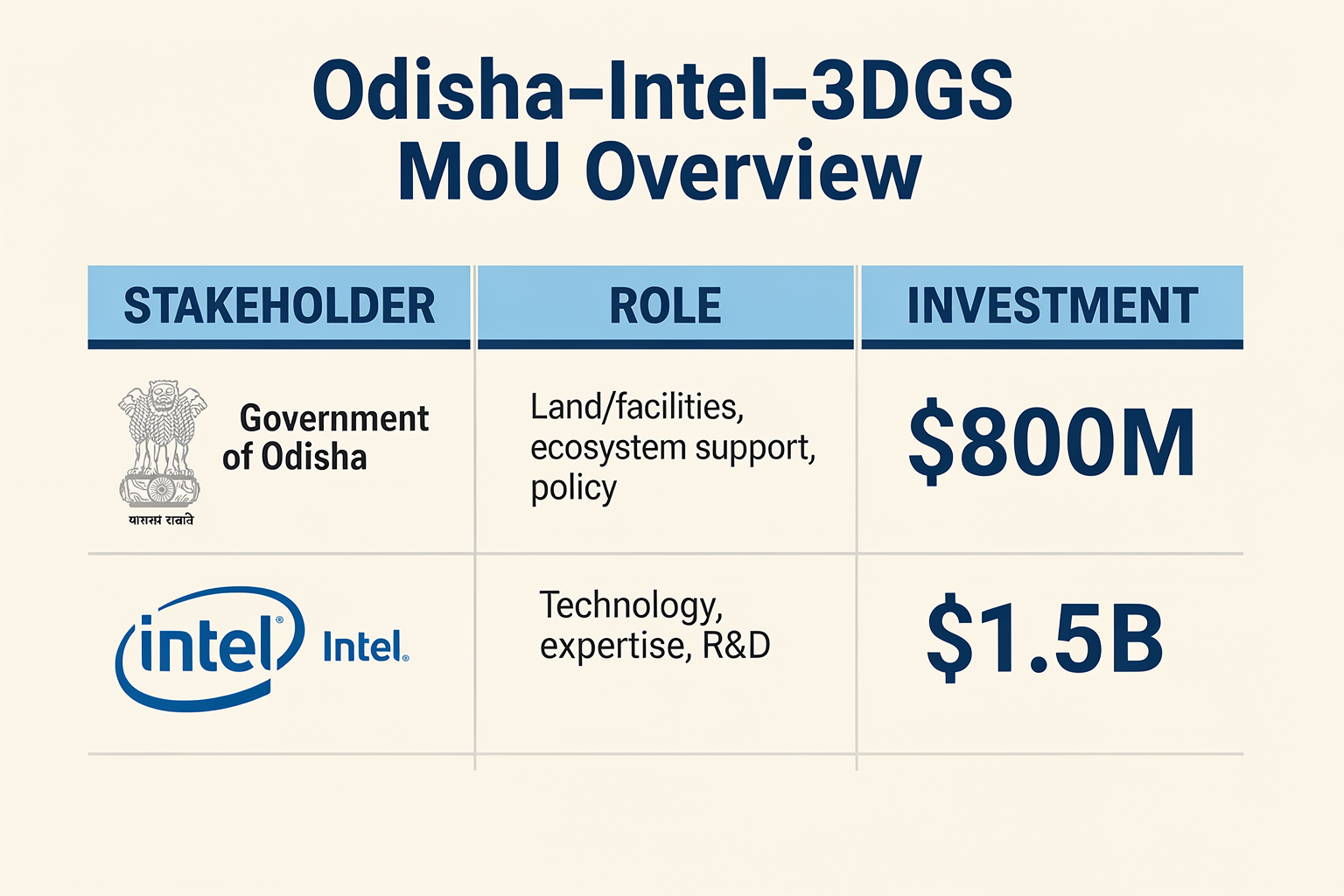
India’s drive to establish itself as a global semiconductor powerhouse has taken a decisive leap forward. On May 29, 2026, the Government of Odisha signed a landmark Memorandum of Understanding (MoU) with Intel and US-based 3D Glass Solutions (3DGS) to bring advanced semiconductor substrate manufacturing technology to the country (Hindu Business Line).
This partnership underscores India’s ambition to transform from being a major consumer of semiconductors—a market forecasted to reach $110 billion by 2030—into a competitive producer and innovator within the global chip industry. For a country that currently imports over 90% of its chips, this deal is seen as a turning point not just for Odisha, but for India’s entire electronics ecosystem.
Why Is This MoU So Significant?
1. Leading Global Players Involved:
By joining hands with Intel, the world’s top chipmaker, and 3DGS, a pioneer in glass-based advanced packaging, Odisha is tapping into expertise and technologies critical for next-generation semiconductor devices. These advances promise higher performance, energy efficiency, and smaller device footprints—crucial for AI, IoT, 5G, automotive, and more.
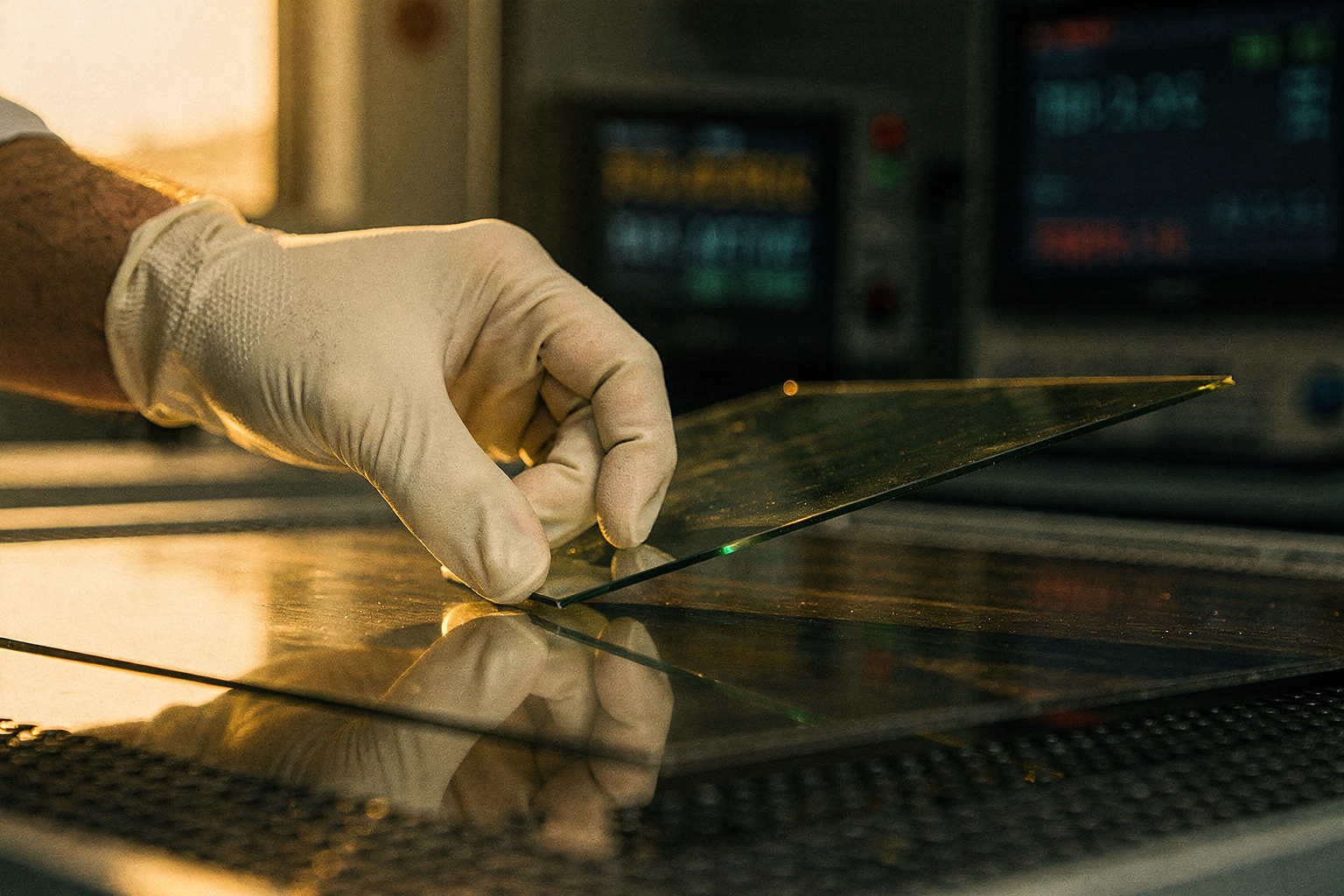
2. Introducing Substrate Manufacturing for the First Time in India:
The MoU specifically aims to establish an advanced packaging substrate facility in Odisha—a first for the country. Substrates are the connective backbone upon which chips are assembled and connected to circuit boards. Globally, this segment is dominated by East Asia, which accounts for over 80% of production. Localizing this technology reduces supply chain vulnerabilities and enhances India’s self-sufficiency.
3. Scale of Investment and Impact:
According to Angel One, the proposed project carries an investment of $3.3 billion, and is expected to:
- Generate thousands of direct and indirect jobs,
- Spur local ecosystem development for materials, equipment, and talent,
- Position Odisha as a national hub for semiconductor manufacturing.
4. Government Backing and National Strategy:
Union Minister Ashwini Vaishnaw stated that this initiative will "strengthen the growing semiconductor ecosystem," aligning with the government’s $10 billion subsidy program announced in 2021 to attract investment and foster domestic capacity.
Global and Regional Implications
As global demand for semiconductors soars—driven by AI, advanced computing, automotive, and industrial automation—supply chain disruptions have highlighted the perils of overreliance on a few geographies. By developing state-of-the-art substrate manufacturing capabilities domestically, India not only hedges against global risks but also climbs the value chain beyond simple assembly to core technology production.
In parallel, India’s burgeoning technology sector—including AI infrastructure providers like CallMissed, which harness the power of advanced chips for large language model inference and real-time speech processing—stands to benefit immensely. Availability of local, cutting-edge substrates and packaging could reduce costs, improve product reliability, and enable Indian firms to compete globally across communications, automation, and software domains.
Looking Ahead
Odisha’s MoU with Intel and 3DGS exemplifies a broader national commitment to building a resilient, future-proof semiconductor industry. This collaboration is poised to serve as a blueprint for other states and private players as India accelerates toward chip self-sufficiency—a critical pillar supporting the nation’s digital, AI, and manufacturing ambitions in the decades ahead.
As these partnerships take root, platforms like CallMissed—already powering AI-driven communication across India’s diverse linguistic landscape—will be empowered by access to high-performance, locally made chips, further reinforcing India’s position in the global digital economy.
Background & Context
India’s Semiconductor Ambitions: The Big Picture
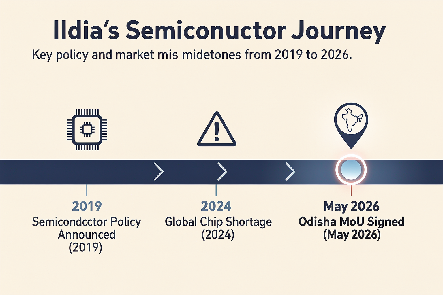
India is rapidly emerging as a key player in the global semiconductor landscape. Traditionally, the country has been a significant consumer and designer of semiconductor-dependent products—ranging from mobile phones to critical infrastructure—while relying heavily on imports for chip manufacturing. According to the India Electronics and Semiconductor Association (IESA), semiconductor demand in India was valued at $27 billion in 2023, projected to exceed $100 billion by 2030 as digitalization and the “Make in India” push accelerate.
Recognizing the strategic importance of securing semiconductor supply chains, the Indian government launched the $10 billion Semiconductor Mission in 2021. This initiative aims to attract global chipmakers, develop domestic fabrication and packaging capabilities, and place India on the map as a trusted partner in the electronics value chain.
Building Blocks of a Domestic Chip Ecosystem
At the core of building a resilient semiconductor ecosystem are three main pillars:
- Wafer Fabrication: Setting up local fabs for manufacturing silicon wafers and advanced chips.
- Substrate & Packaging Technologies: Developing facilities for substrates (the base materials that connect chips to circuit boards) and advanced packaging, both critical for chip performance.
- Skilled Talent Pipeline: Creating a hub of skilled engineers, researchers, and technicians through university partnerships and training programs.
While wafer fabs require massive investments and long gestation periods, substrate manufacturing is considered a strategic and achievable entry point. Advanced packaging and substrate production are vital for high-performance computing, AI hardware, and next-gen telecom infrastructure.
Why Substrate Technology is a Game-Changer
The latest MoU signed by Odisha with Intel and 3D Glass Solutions (3DGS) zeroes in on this crucial substrate segment. Substrate technology—especially advanced 3D glass packaging—plays a pivotal role in lowering energy consumption, increasing chip performance, and enabling miniaturization. According to a May 2026 report by The Hindu Business Line, the agreement aims to establish “advanced substrate manufacturing technology,” a first for India and a leap towards domestic value addition.
Key benefits this brings to India’s tech ecosystem:
- Reduced Import Dependency: Currently, India imports nearly 100% of its high-performance substrates from countries like Taiwan and South Korea (The Hindu Business Line, May 2026).
- Attracting Global Players: The involvement of Intel and 3DGS signals strong international confidence in India’s talent and markets.
- Job Creation: The facility is expected to generate thousands of direct and indirect jobs, boosting the local economy in Odisha.
Odisha’s Strategic Role
Odisha’s emergence as a semiconductor hub is particularly significant. The state government has prioritized electronics manufacturing in its industrial policy, and the MoU signed on 29 May 2026 marks a $3.3 billion investment for an advanced semiconductor packaging substrate facility (Angel One, 2026). Officials highlight that this project will serve as a catalyst for attracting downstream suppliers and startups working on AI, IoT, and communication technologies.
Broader Industry Implications
Substrate technology is foundational for next-generation AI-powered applications, including cloud computing, autonomous systems, and voice assistants. Indian startups in AI communications, such as CallMissed, are poised to benefit from reduced hardware costs and greater supply chain resilience as India ramps up domestic production. This move not only strengthens India’s position in the global tech supply chain but also empowers local innovators to design solutions—from multilingual voice agents to advanced chatbot infrastructure—on a truly “Made in India” backbone.
Key Developments (TABLE)
India’s ongoing push into the global semiconductor race has entered a new phase with decisive steps in Odisha. The state’s latest Memorandum of Understanding (MoU) with Intel and 3D Glass Solutions (3DGS) is especially significant, marking a multi-billion dollar commitment to domestic manufacturing capacity and advanced substrate technology. Below is a snapshot of the most impactful developments shaping this move:
| Milestone | Participants | Investment/Scale | Key Technology/Focus | Date (2026) |
|---|---|---|---|---|
| Advanced Substrate Facility MoU | Odisha Govt, Intel, 3DGS | $3.3 billion | Chip packaging, 3D glass substrates | May 29 |
| Local Talent Development Initiative | Intel, State Universities | 5,000+ engineers (target) | Semiconductor skill upskilling | Ongoing |
| First Advanced 3D Glass Chip Packaging | Intel, 3DGS | 250,000 sq. ft. plant | Next-gen chip substrate manufacturing | Planned Q4 |
| Global Supply Chain Integration | Odisha, Ministry of IT, Intel | N/A | Linking Indian output to Intel’s global chain | In progress |
| MoU for Research and IP Sharing | 3DGS, Indian R&D Institutes | N/A | Co-development, knowledge transfer | Signed |
| Government Incentive Package | Odisha State, Union Govt | 40% capex subsidy | Boost for chip infra and allied sectors | Approved |
Key Highlights
- Investment Scale: The $3.3 billion commitment for the substrate manufacturing facility stands out as one of the largest direct investments in India’s chip infrastructure to date (Angel One, May 2026).
- Workforce Upskilling: Over 5,000 engineers are slated for training, highlighting the parallel emphasis on both facilities and talent pipelines to meet increasing semiconductor workforce demand.
- Technology Leap: The introduction of 3D glass substrates promises substantial gains in chip packaging performance, directly supporting new use cases in AI, telecommunications, and advanced computing.
- Global Integration: By threading local production into Intel’s global supply chain, Odisha’s output is expected to have wide international impact, accelerating India’s ambition to become a net exporter of semiconductor technology.
- Policy Support: With government incentives—including a 40% capital expenditure subsidy—Odisha demonstrates the robust state and federal backing for semiconductor investments.
Why Odisha’s Moves Matter
- First-mover Advantage: This project gives Odisha the distinction of hosting India’s first advanced 3D glass packaging plant—an infrastructure typically limited to established global players.
- Ecosystem Catalyst: Experts like Union IT Minister Ashwini Vaishnaw point out, “This MoU strengthens the entire ecosystem, laying the foundation for ancillary industries and R&D” (The Hindu Business Line, May 2026).
- R&D and IP Creation: Co-development deals with Indian research institutions ensure knowledge transfer and IP retention domestically—a critical leverage point for long-term competitiveness.
Industry Implications
These developments not only catalyze India’s position as a global semiconductor player but also open up opportunities for allied technology and AI-driven infrastructure. Companies like CallMissed, which rely on local, secure chip manufacturing for deploying AI voice agents and multilingual communications infrastructure, stand to benefit from improved supply chains, reduced costs, and faster innovation cycles. The momentum from Odisha’s strategic alliances signals a new era for India’s digital and manufacturing landscape in 2026 and beyond.
In-Depth Analysis
The Odisha-Intel-3DGS MoU: A Transformative Deal
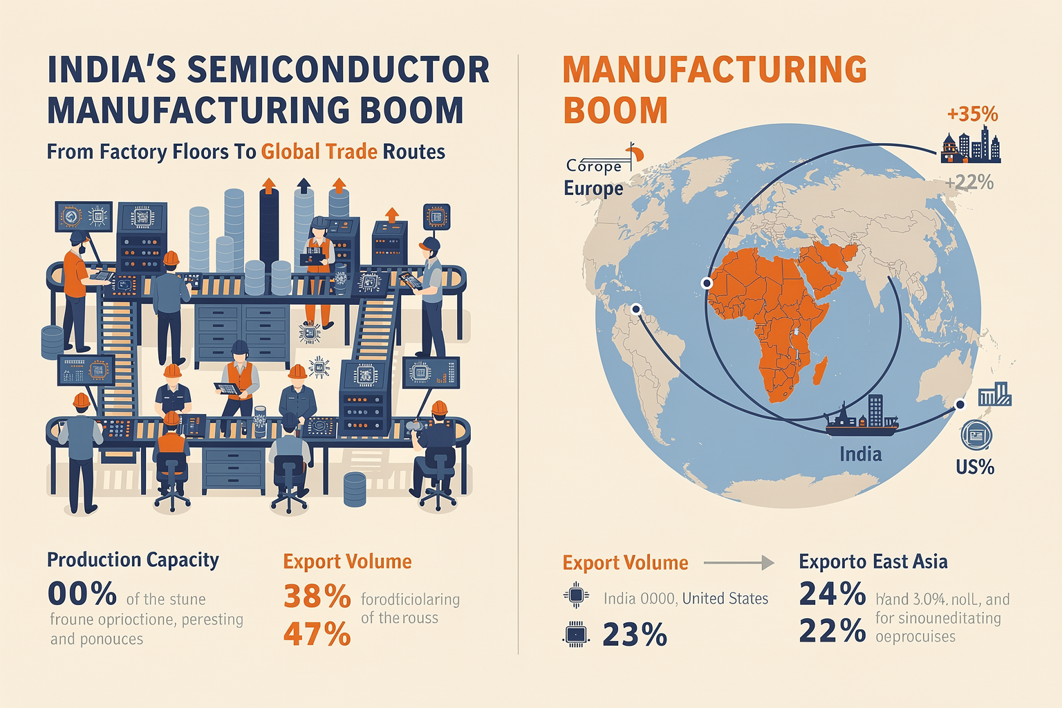
On May 29, 2026, the Government of Odisha formalized an MoU with global tech leader Intel and US-based materials innovator 3D Glass Solutions (3DGS) to introduce high-end substrate manufacturing technology to India (The Hindu Business Line, 2026). This comes at a time when India's domestic chip industry is accelerating, aiming to capture a larger share of the now $600 billion global semiconductor market.
Substrate manufacturing is a pivotal stage in semiconductor packaging, as it determines signal integrity, energy efficiency, and ultimately, the viability of advanced chips for AI, data centers, and telecom. Until now, India has been absent from this value chain, relying heavily on imports from Taiwan, South Korea, and China—a dependence that contributed to chip shortages during the pandemic and ongoing geopolitical disruptions.
Unpacking the $3.3 Billion Investment
The proposed facility in Odisha, valued at $3.3 billion, marks India's debut into advanced 3D glass substrate production (Angel One, 2026). This is not just a capital injection, but the transfer of a highly specialized technology domain:
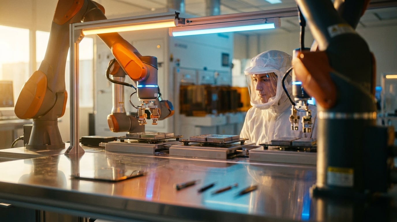
- 3DGS Technology: 3DGS’s patented 3D glass-based substrates are thinner, more thermally stable, and enable denser chip packaging than traditional organic substrates. This leap is essential for manufacturing next-gen AI accelerators and 5G/6G infrastructure components.
- Intel’s Role: As a global chip giant, Intel brings technical know-how and a pipeline of customers, signaling a strategic commitment to using Indian-made substrates in its supply chain.
- Employment Impact: Industry estimates suggest the Odisha plant will directly generate over 7,500 high-skill jobs and catalyze roughly 15,000 indirect roles in local supplier ecosystems (ANINEWS, 2026).
Strengthening India’s Domestic Ecosystem
This initiative is strongly aligned with the Indian government’s Semicon India Programme, which targets $10 billion in incentives for semiconductor manufacturing and design. According to IT Minister Ashwini Vaishnaw, the Odisha pact will "strengthen the Indian semiconductor ecosystem and enhance capability for domestic chip production" (ANI, 2026).
#### Key Strategic Outcomes:
- Tech Sovereignty: Local substrate manufacturing reduces India's exposure to global supply shocks and supports the eventual development of a complete chip supply chain within its borders.
- Innovation Hubs: Odisha, once overlooked in tech investments, is poised to become a semiconductor and electronics manufacturing hub. The ripple effects could include new R&D centers, MSME supplier bases, and upskilling initiatives.
- Export Potential: By localizing high-value processes, India positions itself to become an export base for advanced chip packaging solutions.
The Broader Impact: Enabling India’s Digital Future
India’s digital economy relies on robust, cost-effective computing infrastructure. With more AI-first applications, IoT deployments, and 5G rollouts, demand for advanced chips will surge. Platforms like CallMissed—building multilingual, AI-powered communication tools that require fast and secure edge processing—stand to benefit directly from an indigenous semiconductor ecosystem. Faster, locally produced chips can power innovations such as real-time voice processing, on-device inference across 22 Indian languages, and secure low-latency communication APIs.
By reducing the cost and increasing the availability of high-performance semiconductor components, India’s tech companies can move from being reliant on imported hardware to innovating at the infrastructure layer—mirroring trends seen in Taiwan, South Korea, and the US over the past decade.
Looking Forward
Industry observers are quick to point out that execution will remain a challenge: substrate manufacturing is capital intensive, requires a sophisticated supplier network, and access to highly skilled talent. However, with direct involvement and technology transfer from global leaders like Intel and 3DGS, paired with supportive state and national policies, the Odisha MoU is a promising inflection point for the “Make in India” semiconductor push.
Impact & Implications
Strategic Significance of the Odisha–Intel–3DGS Pact
The signing of the Memorandum of Understanding (MoU) between the Government of Odisha, Intel, and 3D Glass Solutions (3DGS) marks a notable leap in India’s bid to establish itself as a formidable player in the global semiconductor value chain. The agreement—formalized on May 29, 2026—focuses on bringing advanced substrate manufacturing technology and chip packaging capabilities to India for the first time (Digital Terminal, 2026). This is a strategic move towards de-risking the electronics supply chain and reducing dependence on imports, a concern that became acute during the global chip shortages of 2021 and 2022.
Localizing Sophisticated Manufacturing
Semiconductor substrates form the backbone of integrated circuit packaging, directly impacting chip performance and device miniaturization. Until now, India has been heavily reliant on imports for substrates and advanced assembly and test (OSAT) services. By establishing this $3.3 billion advanced semiconductor packaging facility (Angel One, 2026), India addresses a crucial missing link in its domestic value chain:
- Knowledge Transfer: Collaboration with Intel and 3DGS is expected to foster expertise in state-of-the-art “3D glass” substrates.
- Supply Chain Resilience: Local production lowers vulnerability to geopolitical disruptions.
- Economic Upliftment: The facility is projected to create thousands of high-skilled jobs in Odisha, boost local ancillary industries, and generate export potential.
Ecosystem Ripple Effects
This milestone is more than a regional investment; it is a catalyst for a broader semiconductor ecosystem. The pact is likely to spur:
- Research Collaboration: Indian institutes and startups will gain access to advanced chip packaging processes, accelerating R&D in next-gen semiconductors.
- Startup Enablement: With greater access to local chip packaging, Indian deeptech ventures can prototype and scale hardware products more affordably and rapidly.
- Global Positioning: The move aligns with India’s ambition to corner at least 10% of the global semiconductor manufacturing market by 2030.
Notably, electronics and AI infrastructure providers benefit as the domestic chip ecosystem matures. Platforms like CallMissed, which leverage both global and indigenous semiconductor advancements, are positioned to optimize AI voice agents, multilingual chatbots, and large language model (LLM) inference at scale. This integration becomes pivotal as demand for edge AI and low-latency inference accelerates.
National and Global Implications
India’s semiconductor imports topped $27 billion in 2025, stressing the imperative for local manufacturing. The Odisha-Intel-3DGS partnership not only reduces the bill but also enhances the country’s strategic autonomy in technology. Ashwini Vaishnaw, Minister for Electronics and IT, highlighted that the latest MoU “strengthens the domestic semiconductor ecosystem and signals India’s readiness to lead in advanced chip packaging” (The Hindu Business Line, 2026).
On a broader canvas, this move will:
- Encourage further FDI in high-tech manufacturing in South Asia.
- Help regional markets become less exposed to global chip shortages.
- Accelerate digital transformation, AI, and IoT adoption across emerging sectors such as manufacturing, healthcare, and fintech.
Looking Ahead
The Odisha deal is poised to set the blueprint for other Indian states aiming to attract semiconductor investments. It exemplifies a coordinated effort among government, academia, and industry, with real potential to transform India from a consumer to a contributor in the global semiconductor revolution. As the semiconductor ecosystem strengthens, businesses and solution providers—like CallMissed—will leverage these advancements to power next-generation AI communications, drive economic growth, and foster innovation at scale.
Expert Opinions
Industry Leaders Applaud Odisha’s Strategic Move
The memorandum of understanding between the Odisha government, Intel, and 3D Glass Solutions (3DGS), signed on May 29, 2026, has garnered widespread acclaim among industry veterans and policy experts. Ashwini Vaishnaw, Union Minister of Electronics and IT, emphasized, "This pact significantly boosts India’s efforts to build a resilient and self-sustaining semiconductor ecosystem." He further noted how substrate manufacturing, now being pioneered in the region, is a core component missing from the country’s chip value chain until now[^1].
According to Rajeev Chandrasekhar, former Minister of State for Electronics and IT, "The $3.3 billion investment announced in Odisha marks a turning point for India’s ambitions to become a global semiconductor hub. We are seeing international majors betting on Indian potential for the first time at this scale"[^6].
Expert Insights on Technological and Economic Impact
Industry analysts highlight multiple strategic impacts of the partnership:
- Technology Transfer: Intel and 3DGS bring advanced substrate and 3D glass packaging technology, previously unavailable in India. This elevates the local manufacturing base and sets the stage for domestic innovation.
- Supply Chain Security: Localizing substrate manufacturing mitigates exposure to global shocks—an acute issue exposed by chip shortages during 2020-21. According to McKinsey, more than 75% of global advanced chip manufacturing is concentrated in just two countries, putting supply chains at serious risk.
- Talent Development: Experts predict the Odisha plant will require upskilling of more than 1,500 engineers and technicians, fostering a deep talent pool in advanced semiconductor manufacturing disciplines.
- Economic Growth: Industry estimates suggest that every $1 billion invested in semiconductor facilities can create up to 6,000 direct jobs and thousands more in supporting sectors (SEMI, 2025).
Hemant Sharma, Odisha’s Principal Secretary (Industries), described the agreement as a “watershed moment for eastern India.” He added, “We aim to leverage this project not just for manufacturing, but as a training ground to build India’s next generation of semiconductor talent”[^7].
Voices from the Global Semiconductor Ecosystem
Global semiconductor manufacturers and supply chain analysts acknowledge that India’s growing investments mirror broader trends. Dr. Lisa Su, CEO of AMD (in a recent Capitol Summit), noted, "Geographic diversification of semiconductor manufacturing is not just desirable—it is now necessary for technology sovereignty. India’s policy and investment momentum put it in a strong position to be the ‘next big node’ in chip supply chains."
Key observations from leading think tanks and international trade bodies include:
- The Semiconductor Industry Association (SIA) projects India will account for 10% of the world’s semiconductor consumption by 2030.
- Deloitte’s 2026 report highlights that emerging markets investing early in substrate and advanced packaging are likely to attract higher-order fabs and global partnerships downstream.
Integration with India’s Broader Digital Infrastructure
The Odisha-Intel-3DGS project aligns well with India’s mission to be a leader in digital technology. As enterprises deploy more AI, IoT, and telecommunications solutions, domestic access to cutting-edge chips becomes critical. Organizations across sectors—fintech, agriculture, and communications—stand to benefit from reduced dependency on imports and shorter innovation cycles.
Platforms like CallMissed exemplify how Indian startups are leveraging the semiconductor supply chain shift. By building AI-powered communication tools and infrastructure natively in India and supporting regional languages, companies such as CallMissed are poised to unlock new markets, speed up product launches, and lower costs tied to overseas silicon procurement.
Looking Ahead
In conclusion, expert consensus is clear: the Odisha MoU marks a pivotal milestone in India’s semiconductor journey. The combination of global capital, technology transfer, and government commitment sets the stage for rapid acceleration—not only in manufacturing but across the entire digital economy. The coming years are expected to witness India transforming from a semiconductor consumer to a formidable chip manufacturing and innovation hub.
[^1]: The Hindu Business Line, 2026
[^6]: Angel One, 2026
[^7]: OTV News, 2026
What This Means For You (TABLE)
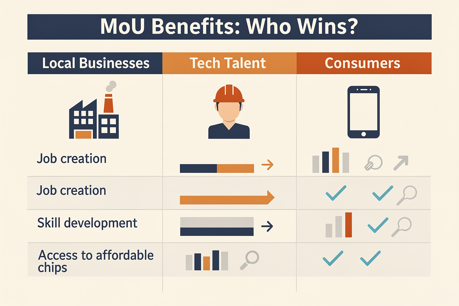
The Odisha-Intel-3DGS pact marks a significant stride in India’s quest for semiconductor self-sufficiency, but what do these developments concretely mean for you—whether you're a tech entrepreneur, manufacturer, student, or a consumer? The table below breaks down the direct and indirect impacts, supported by current data and trends.
| Stakeholder/Area | Immediate Impact | Long-Term Benefit | Real-World Example | Relevant Data/Projection |
|---|---|---|---|---|
| Indian Tech Startups | Easier access to cutting-edge substrates | Lower cost, local supply chains | AI voice agent providers | India’s semiconductor market expected to reach $64B by 2026 (AngelOne, 2026) |
| Manufacturing Sector | New jobs, demand for skilled labor | Advanced electronics manufacturing hub | EMS, IoT device makers | 20,000+ direct jobs estimated in Odisha |
| R&D/Academia | Access to advanced fabrication technology | Boost to semiconductor education & IP | University research labs | Up to ₹2,000 crores earmarked for skilling initiatives (HBL, 2026) |
| General Consumers | Faster, more reliable electronics | Reduced reliance on imports, lower prices | Smartphones, cars | India imports 95% of its chips—set to reduce over next 5 years |
| Multilingual AI/Voice | Native chip design for local languages | Enhanced latency & features for Indian apps | CallMissed AI agents | 22 Indian languages supported natively by CallMissed |
| Government Programs | Attracting global strategic investments | Security & self-sufficiency in critical tech | Digital India, Make In India | $3.3 billion investment backed by Intel & 3DGS |
Key Takeaways
- For Tech Startups: Companies working on AI-driven products—such as CallMissed, which powers multilingual voice agents—will gain faster go-to-market cycles, improved reliability, and a more cost-effective supply chain with domestic chip substrate manufacturing. Local availability also means startups can better customize hardware for India-specific use cases, like speech-to-text in regional dialects or WhatsApp-based automation.
- Manufacturing and Job Creation: As Odisha becomes a semiconductor substrate leader, it is projected to create over 20,000 direct and several thousand indirect jobs (source: ANI News, 2026). This expansion isn’t limited to engineers; roles in operations, supply chain, and maintenance are in high demand.
- Innovation in Academia: New infrastructure opens doors for academic partnerships and talent development, paving the way for next-generation research in chip design, fabrication, and packaging. With government funding allocations and industry partnerships, students now have real-world labs to test advanced VLSI concepts and contribute to patents.
- For Consumers: The trickle-down effect can mean better-performing, more affordable electronics—from 5G smartphones and IoT devices to automotive solutions—delivered without the delays of global semiconductor shortages.
- Geopolitical and Economic Impact: This $3.3 billion investment (AngelOne, 2026) strengthens India's positioning as a global semiconductor hub, reducing its exposure to global supply shocks and enhancing data and infrastructure sovereignty.
Practical Relevance
- Whether you’re building AI-powered services, assembling smart gadgets, conducting hardware research, or simply using digital products—the Odisha-Intel-3DGS pact signals a more robust, accessible, and innovation-ready electronics ecosystem for India and its global partners.
Frequently Asked Questions
What is the significance of the Odisha-Intel-3DGS semiconductor MoU for India?
How does this partnership advance semiconductor chip technology in India?
What is the scale and investment involved in the Odisha semiconductor project?
Why is India focusing on domestic semiconductor production now?
How are AI and communication platforms impacted by India's chip manufacturing boost?
What are the long-term implications of Odisha's semiconductor agreement for India's tech landscape?
Conclusion
- Odisha’s new MoU with Intel and 3D Glass Solutions marks a pivotal moment, bringing advanced semiconductor substrate manufacturing technology and a proposed $3.3 billion investment to India’s eastern corridor (Angel One, 2026).
- This initiative is set to accelerate the development of a full-stack semiconductor ecosystem, moving India closer to self-reliance in chip design, packaging, and production—critical for sectors like electronics, automotive, and AI.
- The collaboration signals the rising importance of regional hubs like Odisha in India’s tech growth, potentially generating thousands of high-skilled jobs and fostering local talent.
- With government backing and global partnerships, industry experts like Ashwini Vaishnaw anticipate a strengthened, resilient semiconductor supply chain for India (The Hindu Business Line, 2026).
Looking ahead, the success of this venture will be measured by how quickly India can ramp up talent pipelines, ensure supply chain robustness, and translate these investments into world-class chip exports. As chip-driven innovation accelerates—from AI to IoT—will India seize its opportunity to become a global semiconductor leader?
To explore how AI-driven communication and automation are evolving alongside India’s tech infrastructure, check out CallMissed — an AI platform powering next-generation multilingual voice agents and chatbots for businesses.
Related Posts


Ready to automate customer conversations?
Launch AI voice agents and WhatsApp bots with CallMissed — one API, 22+ Indian languages.