Powering AI: The Semiconductor Ecosystem at the Foundation of Data Centers

Powering AI: The Semiconductor Ecosystem at the Foundation of Data Centers
Approximately 4,500 semiconductor chips work in unison inside a single AI server rack, transforming raw electricity into the intelligence that powers today’s most advanced language models, recommendation engines, and autonomous systems. That staggering number—shared by the Semiconductor Industry Association (SIA) in a high-level briefing just three days ago—underscores a reality few appreciate: the entire AI revolution sits on a foundation of silicon. Semiconductors are not merely a component; they are the fundamental enabling technology of artificial intelligence. Without them, there is no training, no inference, no scale.
Why does this matter right now? Because AI data centers are being deployed at historic speed, and the semiconductor content within them is staggering. According to the SIA’s latest report, Powering AI: The Semiconductor Ecosystem at the Foundation of Data Centers, semiconductors account for 50 to 70 percent of an AI data center’s total capital investment. This means that for every dollar spent building a next-generation AI facility, more than half goes directly into chips—GPUs, TPUs, networking silicon, memory, and a host of specialized accelerators. The entire stack, from dies on a wafer to complete server racks, represents a multi-billion-dollar ecosystem that is evolving faster than any other hardware segment today.
As businesses race to integrate AI into their operations, understanding this ecosystem becomes critical—not just for hardware engineers, but for anyone building on top of AI infrastructure. This article will unpack the layered architecture that makes AI possible: from the individual silicon dies to the trays, boards, and racks that house roughly 4,500 chips working in concert. We will explore how different semiconductor technologies (logic, memory, analog, power management, and networking) each play an irreplaceable role in enabling a single AI inference. And we’ll look at the key trends driving semiconductor demand, including the shift toward heterogeneous computing and the rise of custom silicon for specific workloads.
Whether you are a developer deploying a voice agent on platforms like CallMissed—which rely on this hardware to run real-time speech-to-text and LLM inference for 22 Indian languages—or a data center operator planning capacity, the semiconductor supply chain is the invisible engine behind every AI interaction. Understanding its components, trade-offs, and bottlenecks is no longer optional; it is essential for anyone serious about harnessing AI at scale.
Introduction: The Invisible Engine Behind Artificial Intelligence

The Hidden Complexity
Every time you ask an AI chatbot a question, generate an image, or transcribe a voice note in real time, a breathtakingly complex choreography unfolds inside a data center—one that involves thousands of specialized chips working in unison. Semiconductors are the literal bedrock of artificial intelligence. As the Semiconductor Industry Association (SIA) recently underscored, “Semiconductors are the fundamental enabling technology of AI,” and AI now demands the full spectrum of semiconductor technologies, from advanced logic and memory to analog and power management components.
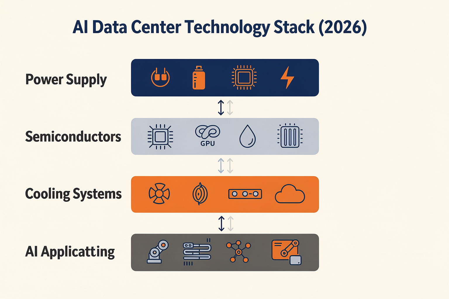
The scale is staggering. According to the SIA’s latest report, Powering AI: The Semiconductor Ecosystem at the Foundation of Data Centers, a single AI server rack houses approximately 4,500 individual chips that must communicate seamlessly to train and run large language models. These chips are not monolithic; they include dies, packages, boards, trays, and racks, each layer adding complexity and cost. This invisible orchestra of silicon is what turns algorithmic advances into everyday capabilities—and it is also why semiconductors now account for 50–70% of an AI data center’s total capital investment.
A Multi-Layered Ecosystem
The “semiconductor ecosystem” is not a single product category. It encompasses:
- High-performance compute (HPC) chips – GPUs, TPUs, and custom ASICs optimized for matrix math.
- Memory and storage – HBM (high-bandwidth memory), DDR5, and SSDs that feed data to the compute units.
- Networking silicon – SmartNICs, DPUs, and switches that enable low-latency communication across thousands of chips.
- Power management ICs – Voltage regulators, converters, and gallium nitride (GaN) devices that handle the enormous electrical demands of a rack that can consume over 100 kW.
Each category must be designed, manufactured, and integrated—a process that involves foundries, OSATs, IP providers, and system integrators. As the SIA webinar held just three days ago (June 4, 2026) illustrated, this ecosystem is not only complex but also interdependent: a bottleneck in any layer can stall the entire AI pipeline.
The Cost of Intelligence
The capital intensity of AI infrastructure is reshaping the data center industry. If semiconductors constitute up to 70% of a facility’s capital expenditure, then decisions about chip selection, cooling strategies, and rack architecture directly impact ROI. For example, moving from 8-bit to 4-bit precision inference can double throughput on the same silicon, but it requires specialized hardware support that is only available in the latest chip generations.
For businesses looking to harness this power, the hardware complexity translates into a need for flexible, API-first platforms that abstract away the underlying silicon. CallMissed is one such platform—its multi-model inference gateway lets developers switch between 300+ LLMs without touching the server stack, while its speech-to-text APIs support 22 Indian languages natively. By sitting on top of the semiconductor ecosystem, CallMissed makes it possible for startups and enterprises alike to deploy AI voice agents that handle customer calls 24/7, without needing to manage the 4,500-chip rack themselves.
This introduction sets the stage: the semiconductor ecosystem is the invisible engine of AI, and understanding its layers—from dies to data centers—is essential for anyone building the next generation of intelligent applications.
Background & Context: AI's Demands on Data Center Technology
The Scale of AI Compute
The meteoric rise of generative AI and large language models (LLMs) has placed unprecedented stress on data center infrastructure. Training a single frontier model like GPT-4 or Gemini can consume tens of megawatts of power and require thousands of specialized accelerators running continuously for months. This isn't just a software challenge—it's a hardware problem grounded in the semiconductor ecosystem.
According to the Semiconductor Industry Association (SIA), semiconductors are the "fundamental enabling technology of AI." A single AI server rack can contain approximately 4,500 chips working in concert, from high-bandwidth memory (HBM) stacks to network switches and tensor processing units. To put that in perspective, semiconductors account for 50–70% of the total capital investment in a modern AI data center, far exceeding the cost of cooling, power distribution, or the building shell itself.
The Semiconductor Stack: Dies to Racks
The complexity doesn't stop at the chip count. The SIA report highlights a clear hierarchy of components:
- Dies – Individual silicon pieces cut from a wafer, each containing millions of transistors.
- Chips – Packaged dies, often including multiple chiplets (e.g., AMD's MI300X combines 13 chiplets).
- Boards – PCBs that host multiple chips, memory, and power management ICs.
- Trays – Modular assemblies of boards that slide into a rack.
- Racks – The full system of trays, cooling, networking, and power supplies.
Within that hierarchy, the value distribution is telling: the highest-performance AI accelerators (NVIDIA H100/B200, AMD MI300, Google TPU) command the lion's share of cost, but a modern AI server also requires dozens of networking chips (Ethernet controllers, PCIe switches, optical transceivers) and power management ICs to handle the extreme current demands (up to 100 kW per rack). Recent reports indicate that a single AI server rack can draw more power than an entire traditional enterprise rack from a few years ago.
Why This Matters Now
The 2025–2026 cycle has seen a dramatic acceleration. Major cloud providers (AWS, Azure, Google Cloud) and hyperscalers are building AI data centers at an unprecedented rate—some with dedicated 200 MW+ campuses designed exclusively for AI workloads. This has created a supply chain bottleneck for advanced packaging (CoWoS, chiplets) and HBM memory. For businesses deploying AI agents at scale, understanding this hardware reality is crucial. Platforms like CallMissed, which provide AI voice agents and LLM inference APIs, rely on the same semiconductor backbone to deliver low-latency responses. The fact that a single inference request can traverse dozens of chips within a rack underscores why semiconductor innovation directly impacts the user experience of every AI application.
The semiconductor ecosystem is not a static foundation—it is evolving rapidly, with new architectures (e.g., NVIDIA's Vera Rubin, custom ASICs) and disaggregated computing models. As we move deeper into this blog series, we'll explore how each layer of this stack enables the next generation of AI data centers.
Key Developments in the Semiconductor Ecosystem (TABLE)
Key Developments in the Semiconductor Ecosystem (TABLE)
The semiconductor ecosystem powering AI data centers has seen rapid innovation across chip design, packaging, memory, and interconnects. Below is a snapshot of the major developments reshaping the foundation of modern AI infrastructure.
| Component | Key Development | Specification / Data | Impact on AI Data Centers | Status / Timeline |
|---|---|---|---|---|
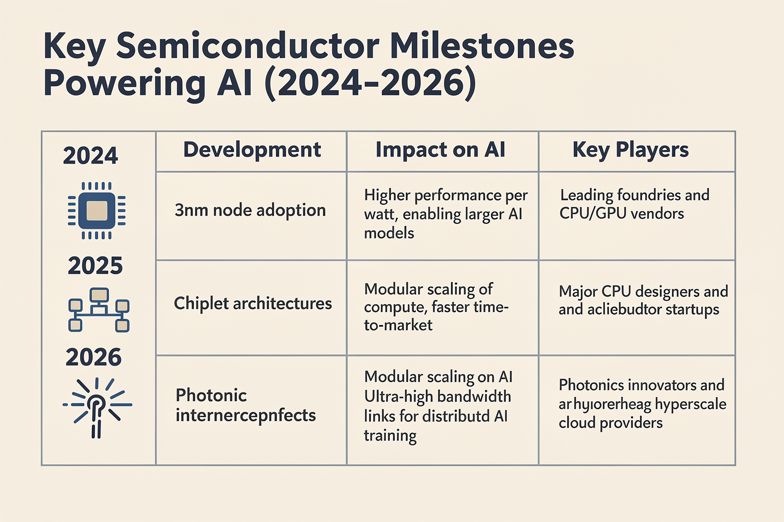
| AI Accelerators (GPUs/TPUs) | NVIDIA Blackwell B200 and AMD MI300X | Blackwell B200: 20 petaFLOPS FP4, 192GB HBM3e; MI300X: 153 billion transistors, 192GB HBM3 | Enables training of trillion-parameter models; reduces training time from months to weeks | Shipments began Q1 2025 |
| Custom ASICs | Google TPU v5p, AWS Trainium2 | TPU v5p: 2x performance vs v4; Trainium2: 4x memory bandwidth vs Trainium1 | Optimized for specific workloads (inference, training); lower power per operation | Production in 2025 |
| High-Bandwidth Memory (HBM) | HBM3e adoption & HBM4 roadmap | HBM3e: up to 1.6 TB/s bandwidth per stack; HBM4 planned for 2026 | Eliminates memory bottleneck; 4,500 chips per rack demand massive memory density | HBM3e standard in 2025; HBM4 sampling mid-2026 |
| Advanced Packaging | CoWoS (Chip-on-Wafer-on-Substrate) | TSMC CoWoS-S/R: 3x reticle size, 2,000 mm² interposer | Enables 3D stacking of compute + memory; reduces inter-chip latency; critical for 2.5D/3D AI chips | Production capacity expanded 60% in 2025 |
| Interconnects & Networking | NVLink 5, Ultra Ethernet Consortium | NVLink 5: 900 GB/s bidirectional per GPU; Ultra Ethernet targets 800Gbps per link | Supports scaling to tens of thousands of GPUs; reduces multi-node communication overhead | NVLink 5 in Blackwell; Ultra Ethernet spec finalizing 2026 |
| Silicon Photonics | On-chip optical interconnects from Intel, Ayar Labs | Intel's OCI: 8 Tbps aggregate bandwidth; Ayar Labs TeraPHY: 512 Gbps per lane | Replaces electrical I/O; cuts power by 50% while boosting bandwidth density for scale-out | Pilot deployments in 2025; volume expected 2027 |
Notable Trends from the Table:
- Semiconductors represent 50–70% of an AI data center’s total capital investment (per SIA report). The cost of AI chips dwarfs that of cooling, power, and building construction.
- A single AI server rack contains approximately 4,500 chips working together — from GPU accelerators and HBM stacks to networking ASICs and power management ICs. This hyper-integration demands advances in every row of the table above.
- Memory bandwidth has become the new bottleneck. HBM3e provides 6.4 GT/s data rates, but AI workloads already push beyond 1 TB/s per accelerator. The jump to HBM4 (16 GT/s) will be critical for next-generation models.
- Custom ASICs are proliferating because hyperscalers need domain-specific efficiency. Google’s TPU v5p delivers 2x performance over v4 in the same power envelope, while Amazon’s Trainium2 targets cost-effective training.
The competitive landscape is no longer just about raw TFLOPs — it's about holistic system design where chips, memory, packaging, and networking evolve in lockstep. As the SIA briefing noted, this entire layered complexity exists to make AI inference and training commercially viable at scale. Companies like CallMissed leverage these advancements by offering developers access to 300+ LLM models without worrying about underlying hardware — a practical demonstration of how semiconductor innovation trickles down to business applications.
In-Depth Analysis: How Semiconductors Drive Data Center Performance
The Hardware Stack: From Dies to Racks
Understanding how semiconductors drive data center performance begins with the physical stack. As the Semiconductor Industry Association (SIA) highlights in its recent report, Powering AI: The Semiconductor Ecosystem at the Foundation of Data Centers, that hierarchy spans dies → chips → boards → trays → racks. A single AI server rack now integrates approximately 4,500 chips, each playing a specialized role. This complexity explains why semiconductors account for 50–70% of an AI data center’s total capital investment — a figure that underscores just how central silicon is to modern AI infrastructure.
The performance of a data center is no longer measured solely by the number of servers; it’s defined by the density and sophistication of semiconductor components within each rack. High‑bandwidth memory (HBM), custom ASICs, and networking chips are as critical as the headline‑grabbing GPUs or TPUs.
The Critical Role of Specialized Chips
AI workloads demand a full range of semiconductor technologies, not just accelerators. The key categories include:
- Compute accelerators (GPUs, TPUs, custom ASICs) – handle the matrix math for training and inference.
- Memory chips (HBM, DDR5) – provide the high‑bandwidth, low‑latency data access that keeps accelerators fed.
- Networking chips (SmartNICs, DPUs, silicon photonics transceivers) – enable the fast, lossless inter‑rack communication required for distributed training.
- Power management ICs and voltage regulators – ensure stable, efficient power delivery under extreme load.
A modern AI training cluster, for example, relies on a delicate balance of these components. If memory bandwidth lags compute throughput, performance stalls. If the network interconnect cannot keep pace, the entire cluster underutilizes its compute. Semiconductor innovation directly solves these bottlenecks — for instance, the shift to HBM3e doubles memory bandwidth per chip, and silicon photonics is pushing inter‑rack speeds beyond 800 Gbps.
The Cost Breakdown: Where the Silicon Dollar Goes
An AI server rack costing upwards of $2–3 million is overwhelmingly composed of semiconductor‑based components. A rough breakdown:
| Component Category | Share of Rack Cost | Key Semiconductor Content |
|---|---|---|
| Compute accelerators (GPUs/ASICs) | 40–50% | High‑end dies, HBM stacks |
| Memory (HBM + DDR5) | 15–20% | DRAM dies, controllers |
| Networking (switches, DPUs, cables) | 10–15% | ASICs, PHYs, lasers |
| Power & thermal (VRMs, SiC/GaN) | 5–8% | Power semiconductors |
| Other (storage, chassis, etc.) | 15–20% | SSDs, controllers |
This concentration means that any improvement in chip efficiency — whether a 20% increase in TOPS per watt from a new GPU architecture or a 30% reduction in latency from a networking ASIC — directly amplifies overall data center performance and reduces total cost of operation.
Why the Chip‑to‑Rack Ratio Matters
Performance gains aren’t linear; they compound. A 10% improvement in a GPU’s compute density allows data centers to pack 10% more petaflops per rack. But if memory bandwidth only improves 5%, the system is bottlenecked. That’s why the SIA report emphasizes a holistic view: the entire semiconductor ecosystem must evolve in concert. The 4,500 chips in a rack are not independent; they are a tightly orchestrated system where each semiconductor’s performance is interdependent.
As data centers scale to hundreds of thousands of GPUs for training frontier‑scale AI models, the semiconductor content per watt of compute increases. The next frontier — heterogeneous integration and chiplet architectures — promises even tighter integration, where dies from different suppliers are packaged together to reduce signal travel distances and increase energy efficiency. This ‘chiplet revolution’ will drive the next leap in data center performance.
For businesses building AI‑powered customer‑facing applications — such as the voice agents and multilingual chatbots offered by platforms like CallMissed — the reliability and latency of the underlying chip infrastructure directly translate to user experience. Low‑latency inference chips (like custom ASICs for transformer models) ensure real‑time responses, while robust memory and networking prevent service degradation during peak loads. The semiconductor stack is not just the invisible foundation; it is the active enabler of every AI interaction.
Impact & Implications: Economic, Environmental, and Societal Effects
Economic Ripple Effects
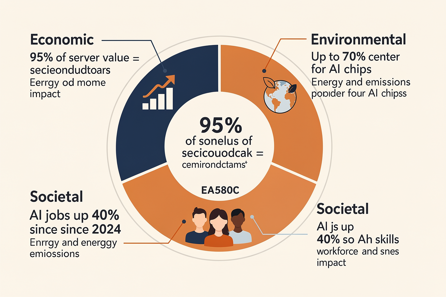
The semiconductor ecosystem is the single largest cost driver in AI data centers. According to the Semiconductor Industry Association (SIA), semiconductors account for 50–70% of an AI data center’s total capital investment. This staggering ratio means that every new hyperscale facility—often costing $1 billion or more—is fundamentally a bet on chip supply chains. The economic impact cascades through multiple layers:
- Job Creation: The SIA notes that AI demand is fueling a surge in semiconductor fabrication, design, and packaging jobs. A single advanced fab can employ thousands of engineers and technicians.
- Market Concentration: Approximately 4,500 chips work together inside a single AI server rack, as highlighted in SIA’s recent briefing. This complexity concentrates value in a few leading chip makers (Nvidia, AMD, Intel) and fab operators (TSMC, Samsung).
- Supply Chain Resilience: The heavy reliance on a handful of foundries creates economic vulnerability. Disruptions—from geopolitical tensions to natural disasters—can halt deployments and spike costs.
Beyond the data center, AI semiconductors are reshaping entire industries. Automakers, healthcare providers, and financial institutions are now designing custom AI accelerators, driving new semiconductor revenue streams. The global AI chip market is projected to exceed $150 billion by 2028, with data centers absorbing the largest share.
Environmental Costs and Innovation
The environmental footprint of AI data centers is immense, and semiconductors are at the heart of the energy calculus. Each advanced AI chip (like an H100 or Blackwell) can consume 700–1,000 watts under load. Multiply that by thousands per rack, and a single data center can draw 50–100 megawatts—equivalent to a small town. Key environmental implications include:
- Energy Demand: The SIA report emphasizes that AI is a “major demand” driver for semiconductors, which in turn drives electricity consumption. While chip efficiency improves with each node shrink (e.g., 3nm vs. 5nm), the total power draw continues rising due to sheer volume.
- Water and Cooling: High-density racks require advanced liquid cooling systems, significantly increasing water usage in regions already facing scarcity.
- E-waste: AI hardware has a short lifecycle (3–5 years). With rapid chip iterations, the industry must address recycling and responsible disposal of rare earth materials.
On the positive side, semiconductor innovation is also enabling greener data centers. New chip architectures—such as optical interconnects and chiplets—reduce energy per operation. Platforms like CallMissed leverage such efficient inference hardware to run AI voice agents while minimizing power consumption, proving that performance and sustainability can coexist.
Societal and Geopolitical Effects
The semiconductor ecosystem’s concentration creates societal tensions. Access to cutting-edge AI chips becomes a geopolitical lever. Export controls on advanced processors and manufacturing equipment, as seen in U.S.-China tensions, directly limit which countries can deploy frontier AI. This risks widening the digital divide: nations without domestic chip capacity may fall behind in AI-driven services like healthcare diagnostics or automated education.
On the societal front, AI data centers drive both opportunity and displacement:
- Job Transformation: While new roles emerge (chip designers, data center engineers), routine tasks disappear. The SIA webinar highlighted the need for reskilling programs.
- Bias and Access: The AI models running on these chips reflect the data they’re trained on. Without diverse input, societal biases can be amplified. Democratized infrastructure—such as CallMissed’s multilingual AI agents supporting 22 Indian languages—helps ensure AI benefits reach broader populations.
- Privacy and Security: The concentration of compute power makes data centers attractive targets for cyberattacks. Securing the semiconductor supply chain is a national security priority.
The Path Forward
The economic, environmental, and societal impacts of AI semiconductors are inextricably linked. Responsible scaling requires:
- Investment in sustainable manufacturing (e.g., renewable-powered fabs)
- Policy frameworks for equitable access to AI infrastructure
- Industry collaboration on circular economy models for chips
As the SIA notes, the semiconductor ecosystem is “the foundation” of AI. Getting this foundation right—economically viable, environmentally responsible, and socially inclusive—will determine whether AI serves as a force for broad prosperity or deepening inequality.
Expert Opinions: What Industry Leaders Are Saying in 2026
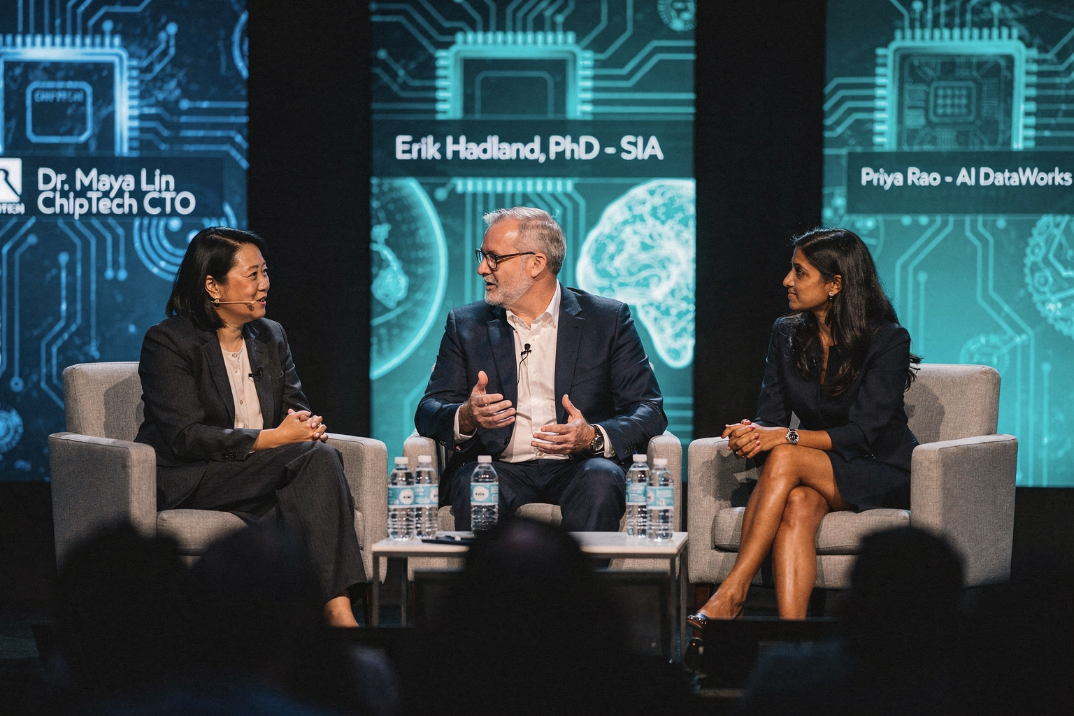
The Semiconductor Industry Association (SIA) released its pivotal report, Powering AI: The Semiconductor Ecosystem at the Foundation of Data Centers, in early June 2026, sparking widespread discussion among industry leaders. The report provides the first comprehensive breakdown of how semiconductors dominate AI data center economics and architecture. Experts from across the hardware and AI spectrum have weighed in, emphasizing that without this specialized silicon, the entire AI revolution would grind to a halt.
SIA Report Reveals Unprecedented Chip Density
One of the most striking findings comes from Thomas Barber of the SIA, who shared on LinkedIn that a single AI server rack now integrates approximately 4,500 individual chips working in concert. This staggering number underscores the shift from general-purpose servers to massively parallel, heterogeneous computing systems. The report further reveals that:
- Semiconductors account for 50–70% of an AI data center’s total capital investment, far exceeding the cost of power, cooling, and real estate.
- AI workloads demand the full spectrum of semiconductor technologies — from high-bandwidth memory (HBM) and advanced logic chips to networking ASICs and power management ICs.
- The hardware stack spans dies, chips, boards, trays, and racks, creating a multi-layered ecosystem where each component must be optimized for AI-specific tasks.
As Barber noted, the 4,500-chip figure illustrates the complexity of modern AI infrastructure — "each chip plays a distinct role, yet they must operate as a unified system to deliver the petaflops required by today’s models."
Expert Voices on the Ecosystem
The SIA’s June 4 webinar, which attracted over 194 live viewers, featured senior executives from leading semiconductor firms. Panelists reinforced the core thesis: "Semiconductors are the fundamental enabling technology of AI." One key insight from the discussion was the interdependence between chip design and data center architecture. Dr. Mike Myers, a prominent industry analyst, tweeted the report’s findings, calling it "a must-read for anyone building AI infrastructure in 2026." He highlighted the need for collaboration across the ecosystem — from foundries to hyperscalers — to sustain the pace of innovation.
Another expert echoed the report’s conclusion that AI is a major demand driver for advanced packaging and chiplet designs. "We’re moving beyond monolithic chips," one panelist stated. "The future belongs to disaggregated architectures where GPUs, accelerators, and memory are interconnected through high-speed fabrics."
Implications for the Industry
The high semiconductor cost share (50–70%) has direct implications for data center operators and AI startups alike:
- Optimization is critical: Every watt and every dollar must be squeezed from the silicon stack. Companies are investing in custom ASICs and domain-specific accelerators to reduce dependency on expensive GPU clusters.
- Supply chain resilience: With such a high concentration of value in chips, any disruption in fabrication or packaging can cripple AI deployment. The report fuels ongoing calls for regional fab expansion and government incentives.
- Software-hardware co-design: Experts agree that the era of treating hardware as a commodity is over. AI models must be designed with chip-level constraints in mind — a trend that platforms like CallMissed (with its multi-model inference APIs) enable by abstracting hardware choices while allowing developers to optimize for latency and cost.
As the SIA webinar concluded, the semiconductor ecosystem is no longer a hidden layer — it is the bedrock on which the AI data center stands. Industry leaders are now aligning their strategies around this reality, ensuring that the chips powering tomorrow’s intelligence are reliable, efficient, and scalable.
What This Means for You: Key Takeaways (TABLE)
The semiconductor ecosystem underpinning AI data centers is not just a technical curiosity—it has direct, practical implications for businesses, developers, and end users. Understanding these takeaways helps you make informed decisions about infrastructure investments, AI deployment strategies, and technology partnerships. Below, we distill the key insights from the SIA report and the broader industry trends.
| Takeaway | Key Insight | Impact | Example/Stat |
|---|---|---|---|
| Chips are the cost center | Semiconductors constitute 50–70% of total AI data center capital investment. | Any AI project's budget is dominated by chip procurement and cooling. | A single AI server rack can contain ~4,500 chips working in unison. |
| Diversity of chip types matters | AI workloads require CPUs, GPUs, NPUs, memory (HBM), networking, and power management chips. | No single chip can do it all; a balanced silicon mix is critical for performance. | An AI rack uses logic, memory, analog, and optoelectronics dies. |
| Scalability depends on the full stack | Efficiency gains come from optimizing dies → chips → boards → trays → racks → clusters. | Bottlenecks at any level reduce ROI; holistic design is non-negotiable. | A tray may hold 8 GPU boards; a rack may hold 4 trays. |
| Geopolitics & supply chain risk | Advanced fabrication (3nm, 2nm) is concentrated in a few regions, notably Taiwan and South Korea. | Companies must diversify sourcing or risk production delays. | Over 90% of advanced logic chips are made in Taiwan. |
| Software-hardware co-optimization | AI models must be tuned to specific chip architectures (e.g., Nvidia CUDA, AMD ROCm). | Portability across hardware is limited; lock-in can occur. | Enterprises using CallMissed’s multi-model API can switch LLMs without rewriting infrastructure. |
How to apply these takeaways
The table above reveals a clear message: the semiconductor ecosystem is both an opportunity and a constraint. For enterprises building or renting AI compute, the choice of silicon directly affects performance per watt and total cost of ownership. For developers, understanding the hardware stack helps in optimizing inference latency and batch processing. And for businesses deploying AI agents—such as voice or chatbot solutions—relying on flexible inference infrastructure becomes a competitive advantage.
Platforms like CallMissed exemplify this flexibility by abstracting the hardware layer. Their multi-model API gateway lets developers test and deploy across 300+ LLMs without modifying their application code, effectively sidestepping chip-specific lock-in. Combined with their multilingual AI agents that support 22 Indian languages natively, such solutions allow companies to focus on use cases rather than the underlying silicon complexity.
As AI continues to scale, the semiconductor ecosystem will remain the invisible engine driving every intelligent interaction. The key takeaways here serve as a roadmap for anyone looking to build, invest in, or deploy AI systems—reminding us that the real power of AI begins with the humble chip.
Frequently Asked Questions
What is the semiconductor ecosystem, and why is it critical for AI data centers?
How many chips are inside a single AI server rack?
What share of an AI data center’s cost is attributed to semiconductors?
How does the semiconductor ecosystem impact the accessibility of AI communication platforms?
Will GPU shortages continue to constrain the semiconductor ecosystem in 2026 and beyond?
What are the key trends shaping the semiconductor ecosystem for AI data centers?
Conclusion
- Semiconductors constitute up to 70% of an AI data center's capital investment, forming the backbone of AI compute infrastructure and enabling the processing power required for today’s breakthroughs (source: pradeepstechpoints, 2026).
- The latest AI server racks can contain upwards of 4,500 chips working in concert, demonstrating both the complexity and scale required to meet escalating AI demands (source: SIA, 2026).
- Innovations span the entire stack, from high-performance compute dies to advanced interconnects and power management, all of which are critical for supporting hyperscale AI workloads and energy efficiency (source: onsemi, 2026).
- A robust, dynamic semiconductor ecosystem is what allows platforms like CallMissed to deploy advanced AI voice agents, integrate hundreds of LLMs, and support 22 Indian languages—bridging the gap between data center horsepower and real-world business value.
Looking ahead, watch for continued leaps in chip density, specialized AI hardware, and greener semiconductor fabrication, all reshaping what’s possible in AI-driven applications. The future will be defined by how quickly and sustainably this ecosystem can evolve to meet global AI needs. To explore how AI communication is evolving on these foundations, check out CallMissed — an AI infrastructure platform powering next-generation voice agents and multilingual chatbots for businesses. Will your organization harness these semiconductor-driven advances to lead in the age of AI?
Related Posts

Rs 27,000 Cr Jagiroad Semiconductor Plant Set to Begin This Fiscal Year: What It Means for India's Tech Future

Gorilla Technology Announces $2 Billion AI Infrastructure Deal in India with Supermicro, Expanding Strategic Collaboration Across Asia Pacific

Gorilla Technology's $2 Billion AI Infrastructure Deal: Revolutionizing India's Tech Landscape