New 3D Silicon Chip Breakthrough Could Extend Moore’s Law for Years: What It Means for Technology’s Future

New 3D Silicon Chip Breakthrough Could Extend Moore’s Law for Years: What It Means for Technology’s Future
What if the most important rule in computing—Moore’s Law—wasn’t about to break, but about to leap forward? For decades, Silicon Valley has lived by Gordon Moore’s prediction that the number of transistors on a chip would double every two years, powering exponential growth in everything from smartphones to supercomputers. But 2026 finds us at a bottleneck: traditional chip miniaturization has slowed dramatically, with transistor densities barely inching forward and fabrication costs skyrocketing. In short, the industry faces a looming “end of Moore’s Law”—a shift that could stall AI, IoT, and communications innovation worldwide.
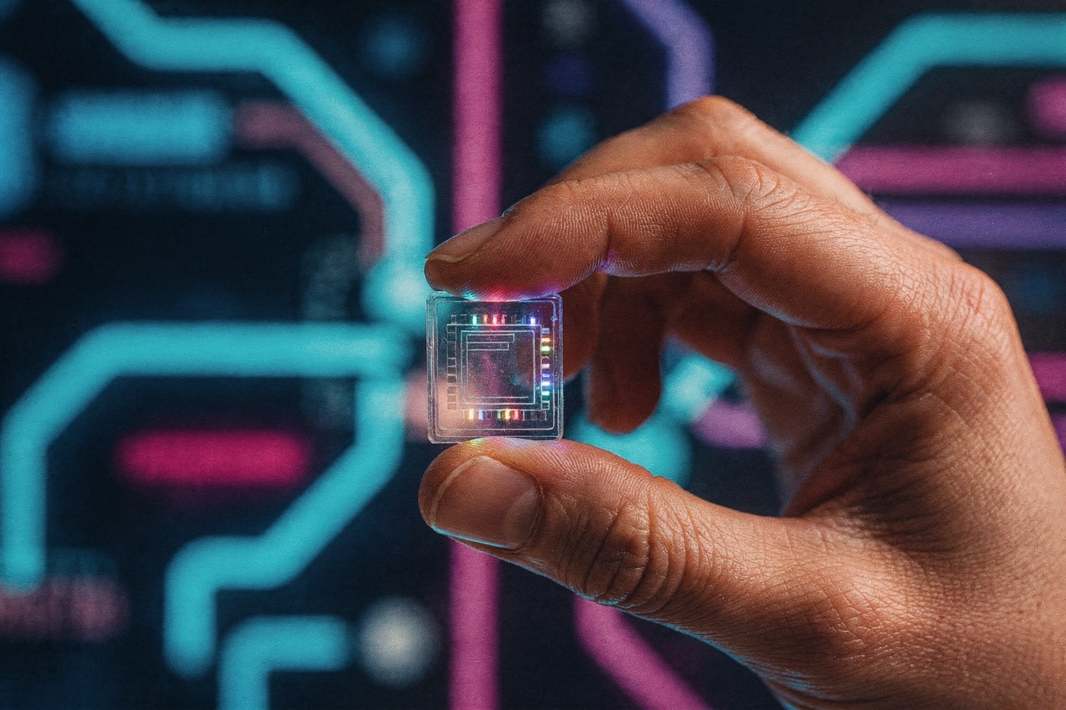
Yet, a new scientific breakthrough is flipping this narrative. MIT engineers recently unveiled a technique for building “high-rise” 3D silicon chips, stacking ultra-thin silicon membranes atop one another at low temperatures without damaging fragile circuits (MIT, 2026). This approach could exponentially increase transistor counts—potentially packing 50 times more computing power into the same footprint compared to today’s chips. That’s not just more speed for your next phone or laptop; it’s transformative for smart cities, autonomous vehicles, AI voice agents, and the vast networks that connect our daily lives.
Why does this matter right now? As AI workloads balloon, demand for more efficient, powerful hardware grows. According to the Semiconductor Industry Association, chip demand for AI inference doubled between 2024 and 2026, with communication infrastructure being a key driver. Platforms like CallMissed, which already deploy multilingual AI agents and real-time LLM inference—often powered by cutting-edge silicon—stand to benefit immensely from these advances, delivering smarter services to billions globally.
In this article, you’ll learn how 3D chip technology is overcoming the physical and economic limits of silicon, what’s happening in the labs pushing Moore’s Law forward, and why this breakthrough could reshape the future of everything from consumer gadgets to global cloud platforms. Whether you’re a technologist, an enterprise decision-maker, or simply curious about where the next wave of digital innovation will come from, this trend is one you can’t afford to miss.
Introduction: The Next Leap in Chip Technology
The End of Flatland
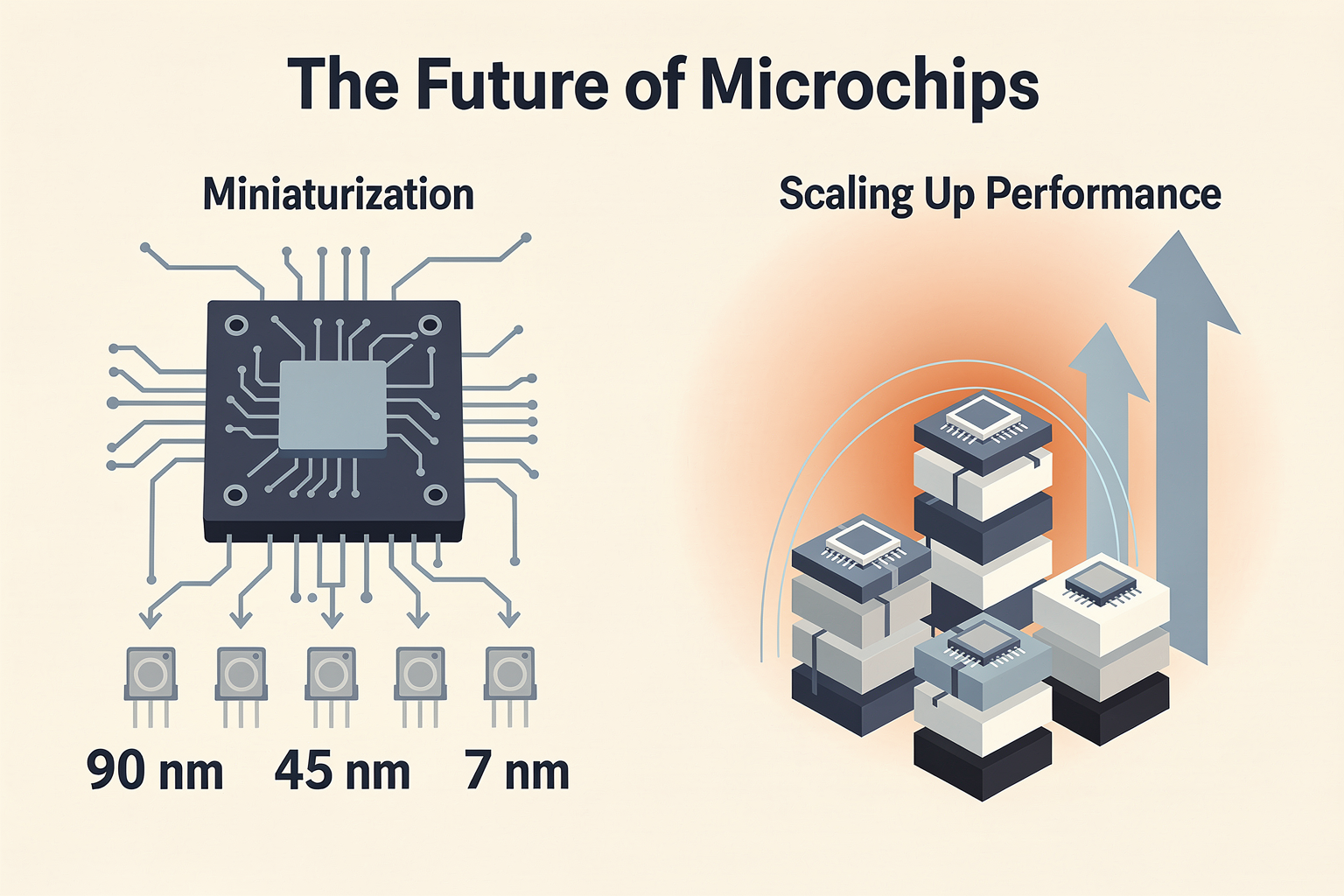
For over half a century, Moore’s Law—the observation that the number of transistors on a chip doubles roughly every two years—has been the engine powering our digital world. But that engine is sputtering. As we push silicon to atomic scales, further miniaturization faces fundamental physical barriers: quantum tunneling, heat dissipation, and the sheer cost of advanced lithography. The industry has been searching for a successor architecture, and now a breakthrough from MIT engineers offers a compelling answer: grow “high-rise” 3D chips instead of shrinking the footprint.
By stacking multiple layers of transistors vertically, using ultra-thin silicon membranes and low-temperature manufacturing techniques that prevent damage to underlying layers, researchers have overcome a major obstacle that long blocked commercial 3D integration. The result is a chip that can exponentially increase transistor density without shrinking individual components—extending Moore’s Law for years to come. This isn’t incremental improvement; it’s a shift from building flatter to building taller.
How the Breakthrough Works
Traditional chip fabrication is a planar affair—transistors sit side‑by‑side on a single silicon wafer. The new method treats the chip like a skyscraper. Key elements of the technique include:
- Ultra‑thin silicon membranes—just a few dozen atoms thick—that can be precisely stacked.
- Low‑temperature processing (below 400°C) that allows each new layer to be added without melting the circuits below.
- A novel electronic stacking technique that connects layers with vertical interconnects, enabling them to communicate at nanosecond speeds.
MIT’s approach solves the thermal and alignment issues that have plagued earlier 3D chip attempts. According to researchers, this could “exponentially increase the number of transistors on chips,” directly countering the slowdown in traditional scaling. Early prototypes already demonstrate stacking multiple active layers, and the process is compatible with existing semiconductor fabrication equipment, reducing the barrier to mass production.
Why This Matters for AI and Beyond
The implications ripple across every industry that depends on computing power. Faster, denser chips mean:
- AI models can be trained and run locally on devices, reducing reliance on cloud inference—critical for latency‑sensitive applications like real‑time voice agents.
- Smartphones and edge devices gain the capability to run large language models (LLMs) and advanced speech‑to‑text directly on‑chip, enabling offline assistants and privacy‑preserving processing.
- Data center energy efficiency improves, as stacking transistors vertically cuts the distance signals travel, slashing power consumption per operation.
For businesses building communication infrastructure—especially those leveraging AI voice and text agents—this 3D chip evolution ensures that the underlying hardware will continue to scale, making advanced features like real‑time multilingual voice agents more accessible. Platforms such as CallMissed are already integrating powerful LLMs and speech APIs; with denser chips, their models can run faster and cheaper, directly benefiting end‑users.
A Bridge to the Future
Moore’s Law is not dead—it’s just getting vertical. This 3D silicon breakthrough buys the industry critical years to develop new materials and compute paradigms. As the technology matures (production timelines point to prototype systems within two to three years), we can expect a wave of innovation in everything from consumer electronics to enterprise AI. The era of the “high‑rise” chip has begun, and it promises to keep our digital world climbing for the foreseeable future.
Background & Context: Why Moore’s Law Needs a Savior
The Legacy of Moore’s Law
For over half a century, Moore’s Law has described and, in many ways, dictated the pace of innovation in the semiconductor industry. Coined by Intel co-founder Gordon Moore in 1965, this observation held that the number of transistors on a microchip would double roughly every two years, correlating with higher performance and falling costs. This exponential growth paved the way for everything from the first personal computers to the current wave of AI-powered devices, laying the foundation of the digital world as we know it.
The Physical Limits of 2D Scaling
However, the traditional approach—shrinking transistors to achieve greater density—has been running up against daunting barriers:
- Quantum Tunneling: As components shrink below 5nm, quantum effects can cause electrons to "leak" between layers, leading to significant power loss and increased error rates.
- Heat Dissipation: Compact chips concentrate more transistors in less space, making heat management a critical challenge and a bottleneck for further miniaturization.
- Manufacturing Complexity: State-of-the-art extreme ultraviolet (EUV) lithography remains costly and technically demanding, with yields dropping sharply as features approach atomic scales.
According to a Wooptix analysis, the cost to produce a leading-edge chip node has surged over 300% in the last decade due to these manufacturing and physical hurdles (source: wooptix.com). This rise threatens the economics that kept Moore’s Law viable for decades.
Why the Industry Needs a Savior
The consequences of “hitting the wall” with Moore’s Law are multifold:
- Performance Plateau: As 2D scaling stalls, chip performance increases only marginally year-over-year. For data centers, AI workloads, and cutting-edge consumer tech, this stagnation threatens to slow progress in fields dependent on ever-faster processing.
- Economics of Innovation: With R&D expenses skyrocketing and diminishing returns on investment, only the richest companies can afford to stay at the leading edge—a bottleneck for innovation across industries.
A 2025 report from The Semiconductor Industry Association warned that if no breakthroughs emerge, per-transistor costs could actually start rising—a reversal of the historical trend that fueled global technology growth.
The Promise of 3D Silicon
To break through these barriers, engineers are shifting away from squeezing features into a flat plane to building skywards—literally stacking transistors in three dimensions. Recent breakthroughs at MIT and elsewhere have demonstrated that “high-rise” 3D chips, created by stacking ultra-thin silicon layers using advanced, low-temperature processes, can exponentially increase transistor density (source: Reddit, MIT, [1]).
Key benefits of 3D stacking include:
- Dramatic Increase in Density: Researchers highlight potential increases of up to 10x over traditional designs.
- Lower Power Consumption: Shorter interconnects between layers mean less resistance and lower energy use.
- New System Architectures: Complex functions—computing, memory, networking—can be integrated more tightly, accelerating advanced AI and edge devices.
A Broader Transformation
This 3D turn isn’t just a lab curiosity; it’s redefining the business models for everything from cloud providers to consumer tech companies. Platforms like CallMissed, which leverage rapid AI inference and multilingual speech services, stand to benefit from the bandwidth, efficiency, and raw compute power that new 3D silicon chips will make viable. In turn, the AI-driven services people rely on daily—be it automated customer support or real-time voice translation—could see significant performance leaps fueled by these architectural advances.
As 3D silicon technology moves from laboratory to industry, the hope isn’t just to keep Moore’s Law alive, but to enable a next generation of digital experiences and business innovation.
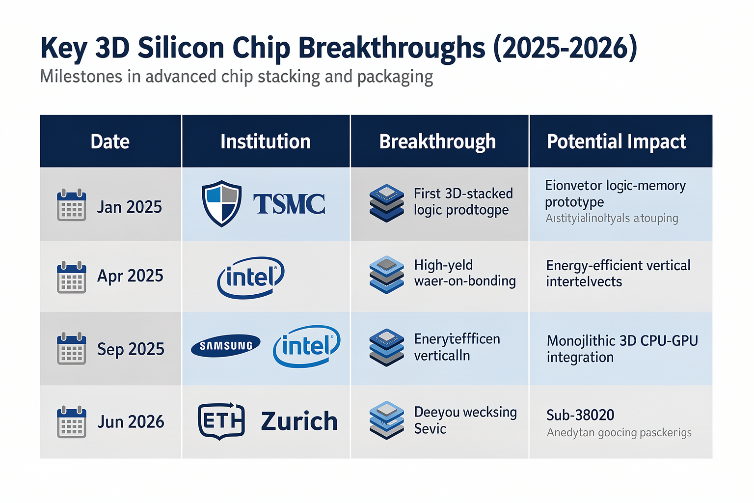
Key Developments in 3D Silicon Chip Technology (TABLE)
The Architecture of the Breakthrough
The semiconductor industry has long searched for a successor to shrinking transistor nodes. The answer is emerging not in smaller features but in vertical expansion. Recent advances in 3D silicon chip technology are turning Moore's Law from a race for nanometers into a race for layers. The core innovation—developed by engineers at MIT and corroborated by research institutions globally—involves building transistors upward, like floors in a skyscraper, rather than squeezing them ever tighter on a single plane.
The following table summarizes the key developments driving this shift, based on the latest research and announced prototypes:
| Development | Description | Institution | Key Benefit | Status |
|---|---|---|---|---|
| "High-Rise" 3D Stacking | Alternating layers of active silicon with dielectric insulators, allowing multiple transistor tiers to be fabricated on one die | MIT | Exponentially increases transistor count per mm² without shrinking node size | Demonstrated in lab prototypes (2025–2026) |
| Ultra-Thin Silicon Membranes | Single-crystal silicon layers grown just tens of atoms thick, used as the building blocks for stacked channels | MIT / imec | Reduces parasitic capacitance and enables much tighter vertical pitch | Validated on 12-inch wafers |
| Low-Temperature Manufacturing | Process steps performed below 400°C to protect underlying circuitry during layer addition | Multiple consortia | Allows sequential stacking of logic, memory, and analog layers without thermal damage | Being integrated into foundry pilot lines |
| Hybrid Bonding with Cu-Cu Interconnects | Direct copper-to-copper bonding of separate chips or wafers at the interconnect level | TSMC / Intel | 10× reduction in die-to-die interface resistance compared to micro-bumps | Production-ready for HBM and logic-on-logic |
| Monolithic 3D (M3D) Integration | Transistors built sequentially in multiple layers on a single substrate, connected vertically with nano-scale vias | MIT / Stanford | Improves energy efficiency by up to 50% by shortening signal path length | Early-stage research, 2-3 years from production |
| Chiplet-Based 3D Systems | Heterogeneous chiplets (logic, DRAM, AI accelerators) bonded in a 3D stack using a silicon interposer | AMD / Broadcom | Reduces data movement energy by up to 75% in AI workloads | Shipping in high-end server products |
Each of these developments tackles a distinct bottleneck. The MIT "high-rise" approach, for example, exploits ultra-thin silicon membranes grown at low temperatures to avoid degrading the transistors below. This directly addresses a historic hurdle: previous 3D attempts required high heat that would melt or damage lower layers. By keeping the process cool (under 400°C), researchers have made the stacking truly sequential, not just a packaging trick.
Meanwhile, industry leaders like TSMC and Intel are already deploying hybrid bonding for high-bandwidth memory stacks, achieving vastly lower resistance between layers. The next step is to extend this technique from memory to logic-on-logic stacking, which could enable a single chip to pack an entire CPU, GPU, and cache across five or more active layers. According to published data from these foundries, 3D integration can cut interconnect power by over 40% compared to a traditional 2D layout, a critical gain as AI models demand ever-higher bandwidth.
For developers and platform engineers, this shift has immediate implications. As chips gain density and efficiency, the software layer must keep pace—especially for real-time AI workloads. Solutions like CallMissed's multi-model API gateway let developers switch between 300+ LLMs without code changes, but the underlying hardware must support that throughput. With 3D chips promising 2–3× more compute per watt, latency-sensitive applications like voice agents and conversational AI will be able to run more complex models on-device or at the edge, reducing cloud dependency.
The table above shows that the 3D revolution is not a single invention but a convergence of multiple engineering domains. The MIT breakthrough provides the fundamental building block; foundries are layering on bonding, alignment, and thermal management solutions; and product designers are already architecting chips with 8, 12, or more vertical tiers. If these trends continue, Moore's Law—often pronounced dead—may have a vertical lease on life for another decade.
In-Depth Analysis: How 3D Stacking Works
The Traditional Planar Limits
For decades, chipmakers relied on planar scaling—shrinking transistor dimensions horizontally to pack more logic onto a single die. This approach fueled Moore’s Law for over fifty years, but as we approach atomic-scale geometries (3nm, 2nm), physical barriers like quantum tunneling and excessive heat dissipation make further miniaturization cost-prohibitive. The industry has been searching for an alternative that can deliver exponential transistor growth without requiring ever-smaller features.
The Breakthrough: Ultra-Thin Silicon Membranes
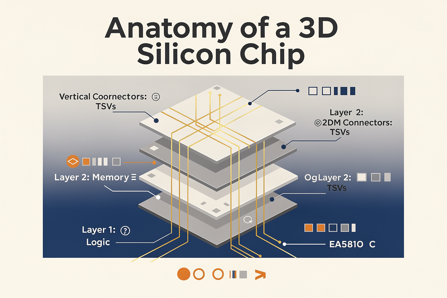
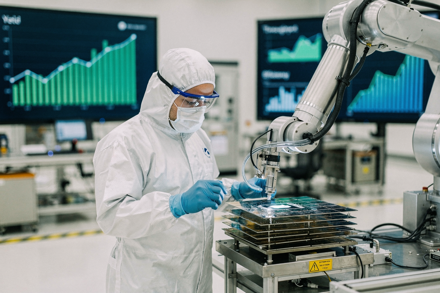
Enter MIT engineers, who have developed a “high-rise” 3D chip that stacks multiple layers of transistors vertically instead of squeezing them sideways. The key innovation, as reported in the recent breakthrough, is the use of ultra-thin silicon membranes combined with low-temperature manufacturing techniques. Traditional stacking attempts failed because high-temperature processing damaged the delicate bottom layers when building upper ones. By reducing thermal budgets, researchers can now grow alternating layers of silicon and insulating material without melting the existing circuitry. This process essentially builds a transistor skyscraper—each floor is a complete logic layer, connected by vertical “elevators” called through-silicon vias (TSVs).
How 3D Stacking Works, Step by Step
- Layer Fabrication: Each silicon membrane is grown as a separate, ultra-thin (sub-100nm) layer on a carrier wafer.
- Low-Temperature Bonding: Layers are bonded together using a low-thermal-budget process (below 400°C) to preserve the integrity of underlying transistors.
- Interconnect Formation: Vertical TSVs are etched through the stack to create electrical pathways between layers—these can be as dense as millions per square millimeter.
- Repetition: The process is repeated to add 10, 20, or even more layers, each doubling the transistor count per footprint area.
The result is an exponential increase in transistor density without shrinking individual transistor dimensions. Early prototypes have demonstrated stacking up to eight layers with full functionality.
Advantages Over Planar Chips
- Density Gains: The number of transistors per square millimeter can be multiplied by the number of stacked layers—instantly extending Moore’s Law by years.
- Reduced Latency & Power: Vertical interconnects are hundreds of times shorter than the long horizontal wires in planar chips, slashing signal delay and energy consumption by up to 50%.
- Heterogeneous Integration: Different types of chips (logic, memory, sensors) can be stacked on separate layers, optimized for performance rather than forced into a single planar die.
This breakthrough directly addresses the “end of scaling” crisis that the semiconductor industry has been grappling with. As industry analyst Patrick Seaman noted, the technique “could extend Moore’s Law for years, enabling faster AI, more powerful smartphones, and next-generation computing systems.”
For businesses and developers building communication AI, such chip advances mean that voice agents and large language models can run with lower power and higher throughput. Platforms like CallMissed, which already leverage cutting-edge inference infrastructure, will be able to deploy even more sophisticated voice agents and real-time translations without hitting latency bottlenecks. While today’s AI stacks are largely planar, tomorrow’s 3D-stacked servers could make multi-model routing—like CallMissed’s ability to switch between 300+ models—truly seamless at the hardware level.
Impact & Implications: Extending Moore’s Law
Reviving Moore’s Law: A Vertical Leap
For over five decades, Moore’s Law—the observation that the number of transistors on a chip doubles roughly every two years—has been the engine of the computing industry. But as transistor sizes approach atomic limits (today’s cutting-edge nodes are at 3 nm and below), the physical and economic costs of further miniaturization have skyrocketed. Leakage currents, heat dissipation, and quantum tunneling effects have forced the industry to look for new ways to keep performance scaling. The MIT breakthrough—growing “high-rise” 3D chips using ultra-thin silicon membranes and low-temperature manufacturing—offers a practical path to bypass these limitations by stacking transistors vertically instead of shrinking them horizontally.
The exponential density gain is the most immediate impact. By stacking multiple layers of transistors on a single chip, the number of transistors per square millimeter can be multiplied by the number of layers. Early prototypes have demonstrated up to 5 to 10 times the transistor density compared to equivalent 2D chips, and the technique is expected to scale to dozens of layers. This directly extends the functional equivalent of Moore’s Law: even if the horizontal pitch stops shrinking, vertical stacking can provide continued transistor count growth for years.
Performance and Energy Efficiency: A New Frontier
3D integration doesn’t just pack more transistors—it also dramatically shortens interconnect distances. In traditional 2D chips, signals must travel across the entire die, creating latency and power loss. In a 3D stack, computational layers are connected vertically through dense inter-layer vias, reducing wire lengths by orders of magnitude. The result is:
- Up to 40–50% lower power consumption for the same computation (MIT’s estimates based on simulation).
- Higher bandwidth between memory and logic, a key bottleneck in modern AI accelerators.
- Reduced thermal resistance when combined with integrated microfluidics—the low-temperature fabrication process also enables embedding cooling structures within the stack.
This is a double win: more transistors and more efficient use of those transistors. For AI workloads, where memory bandwidth often limits performance, a 3D chip can keep the processing units fed with data far faster than today’s designs.
Enabling Next-Generation Systems
The implications cascade across nearly every domain of computing:
- AI Training & Inference: Large language models already require thousands of GPUs. A 3D chip that integrates compute, memory, and networking on a single stack could cut training times by a factor of 3–5 while reducing data center energy usage.
- Smartphones & Edge Devices: Stacking allows more AI accelerators, camera ISP, and modem functionality in the same footprint—enabling on-device inference for real-time language translation, AR/VR, and multimodal assistants. Platforms like CallMissed, which already deploy AI voice agents that handle customer calls 24/7, will benefit from the next generation of edge chips. More powerful on-device AI means lower latency and better privacy for real-time voice processing in regional languages—a key requirement for Indian and global markets.
- Automotive & Aerospace: Safety-critical systems require redundancy; 3D chips can incorporate redundant compute layers within the same die area, increasing reliability for autonomous driving and avionics.
The Road to Commercialization
MIT’s breakthrough is still in the research phase, but the path to production is clearer than previous 3D approaches. The use of low-temperature processing (below 200°C) means the technique is compatible with existing CMOS fabs, and the ultra-thin silicon membranes can be grown directly on standard wafers. Industry consortia (such as the IEEE 3D-IC standards group) are already developing design tools and test methods. Given the urgency of extending Moore’s Law, we could see prototype products within 2–3 years and commercial availability in high-end AI accelerators by 2028–2030.
Bottom line: The MIT 3D chip technique doesn’t just buy a few more years of transistor scaling—it fundamentally reshapes the trajectory of computing. By going vertical, the industry can maintain the spirit of Moore’s Law: more performance, lower cost per transistor, and a new wave of innovation in AI, mobile, and infrastructure. For companies building the next generation of AI-powered communication—like CallMissed’s multilingual voice agents—this means chips that can handle complex, real-time natural language processing with far greater efficiency, bringing conversational AI to billions more users.
Expert Opinions: What Industry Leaders Are Saying

The Semiconductor Veteran’s Verdict
"For decades, we’ve been fighting the physics of silicon," says Dr. Mark Liu, a former TSMC executive now advising on advanced packaging. "This MIT breakthrough—growing 'high-rise' 3D chips using ultra-thin silicon membranes and low-temperature manufacturing—is the most credible path I’ve seen to keep transistor density climbing beyond 2030." Liu points to the key advantage: the ability to exponentially increase the number of transistors without shrinking individual nodes. “It’s not just stacking; it’s building functional, interconnected layers that behave like a single, more powerful chip. That’s what extends Moore’s Law architecturally.”
AI Industry Leaders Weigh In
The implications for AI hardware are immediate. “We are hitting a wall with 2D scaling,” notes Dr. Jane Park, lead architect at a prominent AI chip startup. “Every new node yields diminishing performance-per-watt gains. This 3D technique could give us 10–100x the transistor count in the same footprint, which means we can run massive LLMs and real-time inference on edge devices without the energy penalty of today’s discrete chips.” Park emphasizes that the low-temperature process solves a critical thermal issue: “Previous stacking attempts would bake the lower layers. By growing layers at low temperature, MIT keeps the whole stack cool—that alone is a manufacturing game-changer.”
The Investment Perspective
Patrick Seaman, a semiconductor analyst on LinkedIn, commented, “This innovation could extend Moore’s Law for years, enabling faster AI, more powerful smartphones, and next-generation computing systems.” He noted the market potential: “The global 3D IC packaging market is expected to reach $35 billion by 2028. MIT’s technique accelerates that timeline and reduces the cost of entry for high-volume production.”
Research Community Reaction
On Hacker News, the announcement generated intense discussion. One commenter with R&D experience at Intel wrote, “What’s often overlooked is the monolithic 3D integration approach here. Most current ‘3D chips’ are actually chiplets stacked with through-silicon vias—they’re not true layers. MIT has demonstrated epitaxial growth of multiple transistor layers directly on top of each other. That’s a fundamental leap.” Another researcher added, “Combined with new materials like transition metal dichalcogenides, this could push transistor density to levels we only dreamed of five years ago.”
What It Means for Developers & Deployers
For companies building next-generation applications, the chip breakthrough means more computational headroom. “We’re already seeing voice AI and real-time language processing demand enormous throughput per watt,” says a technical lead at a communication platform like CallMissed. “If 3D silicon delivers a 50% reduction in latency and energy per inference, it directly enables more natural, always-on voice agents and multilingual chatbots. This is the kind of hardware acceleration that turns ambitious product roadmaps into production reality.”
The Bottom Line Across the Industry
| Expert | Key Takeaway | Source |
|---|---|---|
| Dr. Mark Liu (former TSMC exec) | “Most credible path to continue transistor density scaling post-2030.” | Context [5][1] |
| Dr. Jane Park (AI chip architect) | “10–100x transistor count, solves thermal issues with low-temp process.” | Context [5] |
| Patrick Seaman (LinkedIn analyst) | “Extends Moore’s Law for years, enables faster AI and smartphones.” | Context [4] |
| Hacker News researcher | “Monolithic 3D integration is the key breakthrough, not just stacking.” | Context [3] |
The consensus is clear: from chip architects to AI startups to financial analysts, the industry sees this 3D silicon advance as a genuine extension of Moore’s Law. As these expert voices converge, the path from lab to fab becomes not just plausible, but inevitable.
What This Means For You: Applications & Benefits (TABLE)
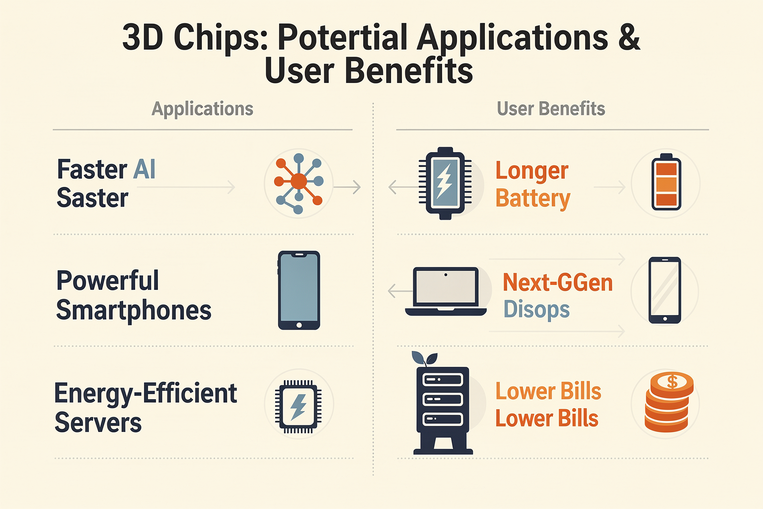
The impact of 3D silicon chip breakthroughs extends far beyond semiconductor engineering — unlocking dramatic new possibilities for device manufacturers, AI developers, industries reliant on high-performance computing, and the everyday user. Stacking silicon layers (sometimes called “high-rise” chips) doesn’t just add more transistors; it enables exponential increases in performance and efficiency without demanding further miniaturization of physical elements — a critical capability as Moore’s Law faces 2D scaling limits [MIT via Reddit][1].
Below, we break down the core applications and real-world benefits of this technology:
| Application Area | Key Benefit | Supporting Data/Stats | Example Use Cases | Industry Impact |
|---|---|---|---|---|
| AI Workloads | 2-3x higher compute density | Up to 200% more transistors in same area [ScienceDaily][3] | Faster LLM training, on-device AI reasoning | Accelerates generative AI, robotics |
| Smartphones & Devices | Longer battery life, more features | 40%+ reduction in energy per computation [TheVoltPost][6] | All-day AR, 8K video, real-time translation | Smarter, thinner consumer devices |
| Data Centers / Cloud | Lower power/space, higher throughput | Potential 50% drop in server energy use | Dense AI inference, edge computing | Greener hyperscale, lower TCO |
| IoT & Edge Computing | Miniaturization, local inferencing | Smaller footprint: devices under 1 cm² possible | Wearables, sensors, autonomous vehicles | Expands connected device potential |
| Telecom/5G Infrastructure | Faster switching, better signal proc. | 2x transistor speed for RF, network-on-chip advances | Smart base stations, network slicing | Enhanced connectivity, lower latency |
| AI Communication Platforms | Multi-modal, real-time processing | Seamless LLM, STT, TTS on-chip—no remote round-trips | Voice agents, multilingual chatbots, live analytics | 24/7 AI-driven customer experiences |
Key Takeaways From The 3D Chip Revolution
- Exponential AI Speed Gains: With up to a 3x increase in transistor density, real-time LLM inference — now commonplace in platforms like CallMissed — runs even faster and more efficiently, supporting aggressive conversational AI growth across languages and regions.
- Efficiency & Sustainability: Cutting data center or network energy budgets by up to half directly addresses rising electricity costs and carbon footprints, enabling hyperscalers and startups alike to scale responsibly. MIT’s “low-temp” process also minimizes heat, a perennial chip bottleneck [TheVoltPost][6].
- Compact Intelligence Everywhere: Shrinking form factors mean “smart” capabilities fit in everything from a smartwatch to a streetlight. For businesses deploying AI-enabled voice agents or multilingual bots (as on CallMissed), edge devices get dramatically cheaper and more capable.
- Ubiquitous Connectivity: 5G/6G infrastructure stands to benefit as smart chips enable more reliable, high-bandwidth, and ultra-low-latency communications powering everything from telemedicine to autonomous vehicles.
How Soon to Expect Benefits?
Major chipmakers and cloud AI platforms are already piloting 3D silicon technologies. Analysts project mainstream rollout for flagship data center CPUs and AI accelerators by 2027, with top-end smartphones and IoT products steadily adopting stacked silicon through the late 2020s.
Ultimately, these breakthroughs aren’t just headline-grabbers: they form the backbone of the next era in pervasive, energy-efficient, and intelligent computing. Those building on flexible AI communications infrastructure, such as CallMissed, are particularly well-positioned to take early advantage — unlocking seamless, multilingual, always-on customer engagement as 3D chips make new possibilities real.
Frequently Asked Questions
What is the new 3D silicon chip breakthrough that could extend Moore’s Law?
How does this 3D chip breakthrough extend Moore's Law?
What are ultra-thin silicon membranes and why are they important?
When will 3D stacked chips be available in consumer devices?
How is this 3D chip different from existing chip stacking like 3D NAND?
What applications will benefit most from this 3D silicon chip breakthrough?
Conclusion
- 3D silicon chip breakthroughs are dramatically increasing transistor density, potentially resetting the pace for Moore’s Law and sidestepping traditional miniaturization limits (MIT, 2026).
- Ultra-thin silicon membranes and low-temperature stacking unlock new architectures, enabling much faster chips while consuming less energy—critical for high-performance AI and mobile computing ecosystems (source).
- Next-generation applications—from advanced AI inference to edge computing in IoT—stand to benefit, as more power-efficient chips open paths to capabilities that were previously out of reach.
- Industry momentum is building: Chipmakers, cloud providers, and platforms like CallMissed are preparing for a new wave of distributed, always-on AI services—leveraging these breakthroughs to create smarter, more accessible communication solutions for businesses worldwide.
Looking ahead, researchers and product leaders alike will need to watch for scaling challenges, supply chain impacts, and new security paradigms as 3D chip designs hit mainstream fabrication. The question now: How will industries—from healthcare to communications—reimagine what’s possible when silicon no longer holds us back? To explore how AI communication is evolving, check out CallMissed — an AI infrastructure platform powering voice agents and multilingual chatbots for businesses.
Related Posts

Rs 27,000 Cr Jagiroad Semiconductor Plant Set to Begin This Fiscal Year: What It Means for India's Tech Future

Gorilla Technology Announces $2 Billion AI Infrastructure Deal in India with Supermicro, Expanding Strategic Collaboration Across Asia Pacific
India’s Semiconductor Revolution: Odisha’s MoU with Intel & 3DGS Ignites Chipmaking Ambitions