
Inside India's Chip Revolution: Minister Ashwini Vaishnaw Unleashes the Next Phase of the DLI Scheme


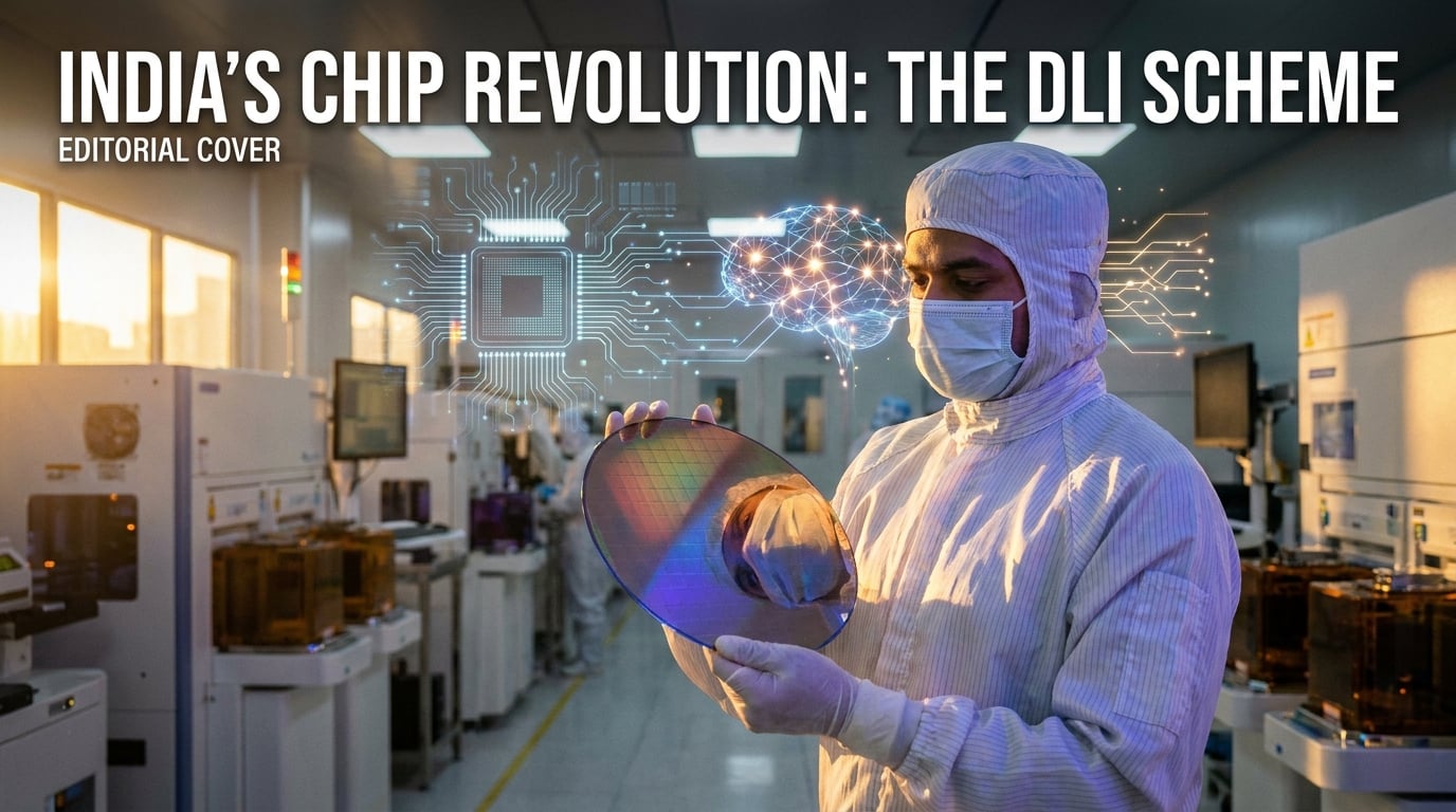
Did you know that a significant portion of the global intellectual property behind advanced microchips is already designed by Indian engineers, yet until...
Inside India's Chip Revolution: Minister Ashwini Vaishnaw Unleashes the Next Phase of the DLI Scheme
Did you know that a significant portion of the global intellectual property behind advanced microchips is already designed by Indian engineers, yet until recently, almost none of those chips bore an indigenous brand? That reality is shifting at a breathtaking pace. India is no longer content with just supplying talent to multinational silicon giants; the nation is actively building its own intellectual property from the ground up. In a landmark move that signals the next aggressive phase of India's Chip Revolution, Union Minister for Electronics and Information Technology, Shri Ashwini Vaishnaw, recently met with 23 semiconductor chip design companies approved under the government’s ambitious Design Linked Incentive (DLI) scheme. This interaction did not just celebrate policy milestones—it showcased a rapidly maturing ecosystem that is poised to disrupt the global semiconductor value chain.
The momentum behind this transition is fueled by concrete, highly sophisticated hardware breakthroughs. At the forefront of this wave is the domestic startup Netrasemi, which has designed India’s first Edge AI System-on-Chip (SoC)—the NETRA A2000—engineered on an advanced 12nm node. This breakthrough is a massive leap forward for sovereign technology. When deployed at a commercial scale, this homegrown chip will power cutting-edge smart vision applications across critical sectors, including autonomous automobiles, intelligent surveillance, and industrial automation.
Why does this focus on Edge AI and local design matter so intensely right now? In an era defined by global supply chain vulnerabilities and geopolitical shifts, technological sovereignty is no longer a luxury—it is a national security imperative. By focusing heavily on "Edge AI"—where data is processed directly on the physical device rather than being sent to distant, energy-hungry cloud servers—India is positioning itself at the absolute frontier of modern computing. This localized processing drastically reduces latency, enhances data privacy, and lowers operational costs, making technologies like autonomous driving and real-time smart surveillance commercially viable at scale.
But Netrasemi is just one success story in a broader, state-backed movement. The government has already approved 24 semiconductor design projects under the DLI Scheme, aiming to catalyze local capabilities in Systems-on-Chip (SoCs), telecommunications, and high-performance computing. To ensure this momentum is sustainable over the next decade, the administration has paired financial incentives with deep academic integration, supporting 240 educational institutions across India with world-class, commercial-grade chip design tools. This dual-track strategy ensures that while startups build the commercial chips of today, the academic pipeline is continuously churning out industry-ready VLSI (Very Large-Scale Integration) designers.
This hardware renaissance is also paving the way for a highly integrated, localized AI ecosystem. As India designs homegrown Edge AI silicon like the NETRA A2000 to process data locally and instantly, AI communication platforms like CallMissed are concurrently revolutionizing the software layer, offering developers production-ready APIs for multilingual Speech-to-Text and voice agents that can natively leverage this emerging local hardware infrastructure.
In this deep-dive article, we will take you inside India's rapidly evolving semiconductor landscape. You will learn how the DLI Scheme is structured to transition startups from design concepts to commercial fabrication, explore the technological specifications and market potential of indigenous chips like the NETRA A2000, and discover how the synergy between academic training and startup incentives is setting the stage for India to become a global chip-design superpower.
Introduction

The global semiconductor landscape is undergoing a monumental paradigm shift, and India is positioning itself at the very epicenter of this revolution. For decades, the nation was recognized primarily as a hub for software talent and back-end IT operations. Today, however, a profound transition is underway: India is rapidly evolving into a global powerhouse for high-value hardware intellectual property (IP) and advanced silicon design.
This transformation was placed under a sharp spotlight during a high-level review meeting where the Union Minister for Electronics and Information Technology, Shri Ashwini Vaishnaw, interacted directly with the leadership of 23 semiconductor chip design startups and MSMEs approved under the central government’s Design Linked Incentive (DLI) Scheme. With 24 design projects officially approved and gaining commercial traction, the meeting served as both a celebration of early technological breakthroughs and a strategic roadmap for India’s self-reliant silicon future.
At the heart of this initiative is a simple but powerful realization: to secure its digital future, India must design the chips that power its infrastructure. By fostering a domestic ecosystem of fabless chip design companies, the government is laying the groundwork for sovereign control over critical technologies, ranging from telecommunications and IoT devices to automotive computing and artificial intelligence.
The DLI Scheme: Moving Up the Semiconductor Value Chain
While building massive semiconductor fabrication units (fabs) requires tens of billions of dollars and years of infrastructure development, chip design is a high-margin, intellectual property-heavy segment where Indian engineers already possess world-class expertise. Historically, this talent was utilized by global multinational corporations. The Design Linked Incentive (DLI) Scheme, a crucial sub-scheme of the ₹76,000-crore India Semiconductor Mission (ISM), aims to redirect this talent toward creating domestic IP.
The DLI Scheme offers financial incentives, design infrastructure support, and deployment assistance to startups and MSMEs engaged in semiconductor design. The objective is to build a robust pipeline of indigenous systems-on-chips (SoCs), application-specific integrated circuits (ASICs), and chipsets.
The approval of 24 distinct projects across various critical sectors—including telecom, smart devices, and high-performance computing—signals that the scheme is delivering tangible, real-world results. By offering up to 50% of eligible expenditure in financial support alongside access to state-of-the-art Electronic Design Automation (EDA) tools, the DLI scheme has effectively lowered the high entry barrier that typically prevents early-stage hardware startups from taking their designs to the tape-out stage.
A Historic Milestone: Netrasemi’s NETRA A2000 Edge AI SoC
Among the most significant breakthroughs highlighted by Minister Ashwini Vaishnaw during the interaction was the achievement of Indian fabless startup Netrasemi. Under the support of the DLI scheme, Netrasemi has successfully designed India’s very first Edge AI System-on-Chip (SoC)—the NETRA A2000—built on an advanced 12nm node.
The technical significance of this achievement cannot be overstated. Designing on a 12nm node requires a high degree of precision, advanced thermal management, and sophisticated architecture. The NETRA A2000 is engineered specifically for Edge AI, meaning it processes complex artificial intelligence algorithms directly on the device rather than sending data back to a centralized cloud server.
When deployed at a commercial scale, the NETRA A2000 will provide high-speed, energy-efficient processing power for a wide range of smart vision applications. These include:
- Surveillance: Enabling real-time, on-device video analytics, facial recognition, and anomaly detection without relying on cloud bandwidth.
- Automobiles: Powering advanced driver-assistance systems (ADAS), object detection, and localized in-cabin AI intelligence.
- Smart Cities: Optimizing traffic management systems, environmental monitoring, and automated industrial inspection pipelines.
By reducing latency, eliminating massive data transmission costs, and enhancing data privacy, indigenous chips like the NETRA A2000 prove that Indian startups are fully capable of competing at the absolute cutting edge of the global fabless silicon industry.
Building the Talent Pipeline: 240 Institutions Empowered
A thriving semiconductor ecosystem cannot survive on financial incentives alone; it requires a continuous, highly skilled workforce. To ensure that India's design capabilities remain globally competitive, Minister Vaishnaw announced that the central government has supported 240 educational institutions across the country with world-class chip design tools.
By integrating industry-standard EDA software and hardware design methodologies into academic curricula, Indian universities are transitioning from theoretical teaching to hands-on, production-grade chip design instruction. This massive educational initiative ensures that thousands of engineering graduates enter the workforce not just as software coders, but as skilled silicon architects, verification engineers, and physical design specialists ready to join the growing ranks of domestic chip startups.
The Synergy of Localized Silicon and Next-Gen AI Infrastructure
The rise of high-performance, domestic Edge AI chips like the NETRA A2000 creates a powerful, symbiotic relationship with the software and AI communication layers. As edge-based compute capabilities become more accessible, the deployment of intelligent, localized software solutions becomes highly practical.
This hardware-to-software integration is where modern communication infrastructure thrives. For instance, platforms like CallMissed—which provides robust AI communication infrastructure, including advanced LLM inference, voice agent systems, and multilingual Speech-to-Text (STT) APIs supporting 22 regional Indian languages natively—stand to benefit immensely from the proliferation of domestic, localized chip designs.
When Edge AI hardware matures locally, AI voice agents, real-time speech translation, and automated customer interaction interfaces can be processed closer to the end-user. This dramatically reduces latency, enhances security, and lowers the computational cost of deploying large language models (LLMs) and real-time communication tools at scale. The alignment of India's hardware ambitions under the DLI scheme with software-driven communication infrastructures like CallMissed represents the ultimate realization of an end-to-end, sovereign, and highly optimized digital ecosystem.
As the India Semiconductor Mission continues to gain momentum, the successful collaboration between policymakers, domestic startups, and academic institutions is turning the vision of an "Aatmanirbhar" (self-reliant) digital economy into a concrete, silicon-based reality.
Background & Context
The Genesis of India’s Semiconductor Ambition
For decades, India has been globally recognized as a powerhouse for software development and IT services. However, the physical hardware powering this digital revolution—the silicon microchip—has historically been designed and manufactured elsewhere. In an era marked by geopolitical shifts, supply chain vulnerabilities, and an exponential rise in demand for computing power, semiconductor self-reliance is no longer just an economic goal; it is a strategic necessity.
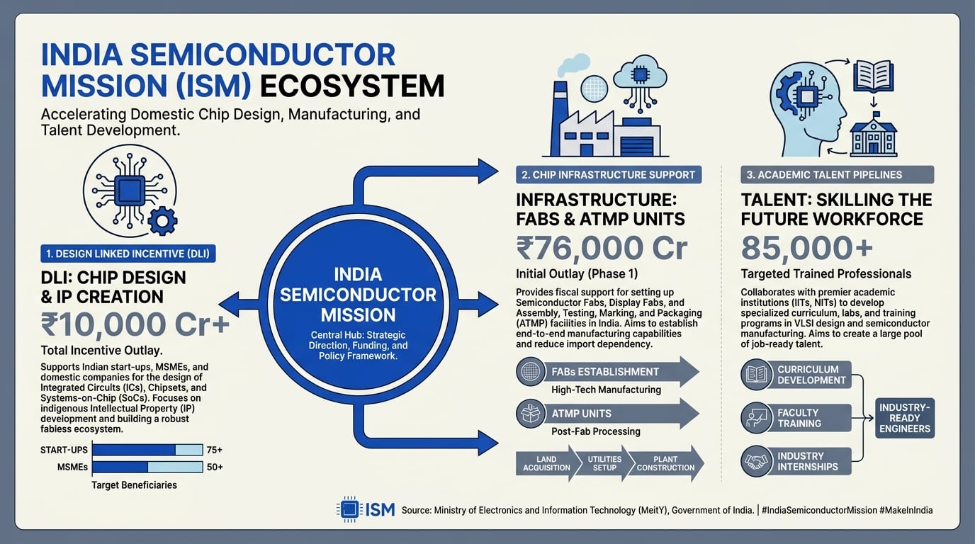
To transition from a consumer of technology to a primary creator, the Government of India launched the India Semiconductor Mission (ISM) with an outlay of ₹76,000 crore. At the heart of this mission lies a critical realization: while building multi-billion-dollar fabrication plants (fabs) is essential for manufacturing, the intellectual property (IP) and highest value-add reside in chip design. By empowering domestic designers, India can control the architecture of the technology defining the next century.
To turn this vision into reality, the Ministry of Electronics and Information Technology (MeitY) introduced the Design Linked Incentive (DLI) Scheme. Recently, Union Minister for Electronics and Information Technology, Shri Ashwini Vaishnaw, met with 23 semiconductor chip design companies in New Delhi to review the progress of the scheme, highlighting how these domestic startups are transforming India's tech landscape from the ground up.
Demystifying the Design Linked Incentive (DLI) Scheme
The DLI Scheme is a forward-looking policy designed to lower the high entry barriers associated with semiconductor design. Developing a chip from scratch requires massive upfront capital, expensive Electronic Design Automation (EDA) tools, and access to fabrication facilities for prototyping—costs that often stifle early-stage startups.
The DLI scheme addresses these challenges by offering financial incentives and infrastructure support across three critical stages of the design cycle:
- Design Infrastructure Support: Under this component, approved startups and MSMEs gain access to state-of-the-art design infrastructure, including EDA tools, IP cores, prototype development support, and testing facilities through the centralized India Chip Centre (C-DAC).
- Product Design Linked Incentive: The government provides financial support of up to 50% of the eligible expenditure, subject to a ceiling of ₹15 crore per application, to assist companies in designing semiconductor products (such as System-on-Chips (SoCs), Systems-in-Package (SiPs), and Application Specific Integrated Circuits (ASICs)).
- Deployment Linked Incentive: To ensure these designs find market viability, the scheme offers an incentive of 4% to 6% of net sales turnover over five years (up to ₹30 crore per application) for semiconductor designs deployed in commercial products.
By de-risking the capital-intensive R&D phase, the DLI scheme encourages local entrepreneurs to create IP that can compete on a global scale, targeting high-growth areas like telecom, automotive electronics, smart wearables, and industrial IoT.
Key Milestones: 24 Approved Projects and the Netrasemi Breakthrough
During the interaction in Delhi, Minister Ashwini Vaishnaw announced that 24 projects have been officially approved under the DLI Scheme, marking a significant acceleration in India's domestic design ecosystem.
A standout success story highlighted by the Minister is Netrasemi, an Indian fabless semiconductor startup. Under the DLI scheme, Netrasemi has successfully designed India’s first edge-native Artificial Intelligence System-on-Chip (SoC)—the NETRA A2000.
- Advanced 12nm Node: The NETRA A2000 is designed on an advanced 12nm technology node, showcasing India's capability to move beyond legacy nodes and design highly complex, power-efficient silicon architectures.
- Commercial Applications: When deployed at scale, this chip will power intelligent, real-time edge processing. This includes smart vision applications across crucial sectors such as:
- Surveillance: Real-time on-device video analytics without relying on cloud servers.
- Automobiles: Advanced Driver Assistance Systems (ADAS) and in-vehicle smart diagnostics.
- Smart Cities & IoT: Distributed sensor processing with minimal latency and high power efficiency.
This breakthrough proves that Indian startups can move from concept to advanced working silicon under structured policy support, establishing a template for the other 23 approved projects currently in various stages of design and tape-out.
The Educational Blueprint: Preparing the Next-Gen Workforce
A thriving semiconductor ecosystem cannot exist without a continuous pipeline of highly skilled engineers. Recognizing this, Minister Ashwini Vaishnaw revealed a massive academic integration program alongside the corporate DLI incentives.
The central government has supported 240 educational institutions across India, equipping them with world-class chip design tools and state-of-the-art laboratory infrastructure. By democratizing access to professional EDA tools—which typically cost hundreds of thousands of dollars per license—the government is ensuring that engineering students graduate with hands-on, industry-ready chip design experience.
This academic push aims to train over 85,000 high-quality engineers in VLSI (Very Large Scale Integration) and chip design technologies over the coming years. This workforce will not only feed domestic startups but will also make India the global talent hub for international semiconductor giants looking to expand their design operations.
Synergizing Hardware Breakthroughs with AI Software Ecosystems
The rise of localized semiconductor designs like Netrasemi’s Edge AI chip directly feeds into India's rapidly growing software and AI ecosystem. As domestic silicon makes edge computing faster, cheaper, and more energy-efficient, developers can deploy sophisticated software architectures directly onto local devices.
This synergy is crucial for modern AI-driven communication infrastructures. For instance, platforms like CallMissed rely on high-performance compute capabilities to deliver real-time AI voice agents, multilingual Speech-to-Text translation across 22 regional Indian languages, and low-latency LLM inference.
When hardware design (incentivized by the DLI scheme) aligns with software innovations, the results are transformative:
- Edge-Native AI Voice Agents: Running AI communication models directly on localized, edge-computing hardware powered by Indian-designed chips reduces latency to milliseconds, making conversations with AI voice agents feel entirely natural.
- Data Sovereignty and Security: Processing sensitive voice and text communication locally on Indian-designed chips ensures that data never leaves the device or the local network, meeting strict security requirements.
- Optimized Localized Models: Specialized chips can be tailored to run lightweight, multilingual LLMs locally, reducing the cloud computing costs that startups often face.
By fostering a self-reliant hardware foundation through the DLI scheme, India is laying the groundwork for a robust, vertically integrated technology stack—where local silicon powers advanced AI communication platforms like CallMissed to deliver seamless, secure, and localized solutions for businesses globally.
Key Developments
The Design Linked Incentive (DLI) scheme, a cornerstone of the India Semiconductor Mission (ISM), has transitioned from an ambitious policy blueprint into a highly productive catalyst for domestic silicon design. During his recent interaction with 23 approved semiconductor design startups and MSMEs, Union Minister for Electronics and IT, Shri Ashwini Vaishnaw, highlighted several critical milestones that underscore India’s rapid evolution from a backend services hub into a hotbed of proprietary semiconductor Intellectual Property (IP).
With 24 design projects approved under the scheme, Indian fabless startups are successfully targeting high-value verticals, including telecommunications, cybersecurity, automotive electronics, and artificial intelligence. The progress achieved under the DLI scheme reflects a highly structured approach to building a self-sustaining electronics ecosystem.
Key Milestones under the DLI Scheme
The table below outlines the core developments, specifications, and infrastructural pillars driving India’s semiconductor design revolution:
| Key Development Area | Technical & Operational Specifications | Target Verticals | Strategic Significance |
|---|---|---|---|
| NETRA A2000 SoC | Developed by Netrasemi; engineered on an advanced 12nm node | Surveillance, automotive AI, smart vision, IoT | India's first domestic Edge AI System-on-Chip (SoC) |
| Project Approvals | 24 projects approved across 23 domestic companies | Telecom, high-performance computing, smart energy | Establishes local ownership of critical silicon IP |
| Academic Enablement | 240 educational institutions equipped with EDA tools | VLSI education, academic research, workforce training | Creates a sustainable pipeline of high-caliber chip designers |
| Incentive Structure | Financial support up to 50% of eligible expenditure | Startups, MSMEs, and early-stage design houses | Lowers the immense capital barriers of chip tape-outs |
| Infrastructure Access | Centralized access to state-of-the-art prototyping & testing labs | Fabless developers, hardware innovators | Accelerates the transition from RTL design to physical silicon |
The Edge AI Breakthrough: Analyzing the NETRA A2000
The standout achievement highlighted by Minister Ashwini Vaishnaw is the design of the NETRA A2000 by Indian chip-design firm Netrasemi. Developed on an advanced 12nm (nanometer) process node, the NETRA A2000 represents a monumental leap forward for India's domestic design capabilities.
Fabricating chips on a 12nm node requires highly sophisticated physical design, synthesis, and verification methodologies. By successfully executing this design, Netrasemi has proven that Indian startups can move beyond mature process nodes (such as 180nm or 65nm) and compete in the deep-submicron territory where modern Edge AI operates.
The primary target for the NETRA A2000 is smart vision technology. When deployed at scale, this system-on-chip will power:
- Next-generation surveillance: Enabling real-time, on-device video analytics, facial recognition, and anomaly detection without relying on latency-heavy cloud servers.
- Automotive ADAS: Providing low-latency processing for advanced driver-assistance systems, where microsecond delays in object detection can impact passenger safety.
- Smart IoT Devices: Empowering industrial and consumer IoT hardware with local, privacy-centric machine learning capabilities.
This breakthrough in Edge AI hardware matches a broader industry trend where computing is shifting from massive centralized data centers directly to the edge. As these domestic chips enter commercial deployment, they will require a highly optimized, localized software layer to unleash their true potential. For instance, communication infrastructures like CallMissed are built to leverage these emerging hardware capabilities. By integrating multi-model API gateways—allowing developers to switch between over 300+ LLMs—and utilizing advanced Speech-to-Text models that natively support 22 regional Indian languages, platforms like CallMissed are ready to run next-generation, ultra-low-latency voice and communication agents directly on local Edge AI silicon as it reaches mass production.
Democratizing Silicon Design: Supporting 240 Academic Institutions
While commercial breakthroughs like the NETRA A2000 capture headlines, the government is simultaneously addressing the foundational talent bottleneck. The semiconductor design process is notoriously capital-intensive, with Electronic Design Automation (EDA) software licenses costing hundreds of thousands of dollars per seat annually. This financial barrier historically kept state-of-the-art tools out of reach for the vast majority of Indian engineering students.
By equipping 240 educational institutions across India with world-class chip design tools (provided by global EDA giants like Synopsys, Cadence, and Siemens EDA), the Ministry of Electronics and Information Technology (MeitY) has democratized semiconductor education. This initiative ensures that:
- Industry-Ready VLSI Engineers: Graduates entering the workforce are already proficient in industry-standard RTL (Register-Transfer Level) design, physical design, and verification flows, drastically reducing corporate onboarding times.
- Academic Innovation: Universities can now actively engage in research-level tape-outs, building niche IPs in areas like analog mixed-signal design, power management integrated circuits (PMICs), and RF (Radio Frequency) systems.
- Decentralized Talent Pool: By spreading these tools across 240 campuses, the government is shifting the chip design talent pool beyond tier-1 metro areas, fostering a geographically diverse workforce.
From GDSII to Commercialization: The Road Ahead
Designing a chip is only half the battle. Once a design house produces the final GDSII file (the database format containing the physical layout of the integrated circuit), it faces the complex challenge of fabrication, packaging, and commercialization. Currently, Indian fabless startups must secure fabrication slots with international foundries.
However, the DLI scheme’s comprehensive approach—providing financial incentives for prototyping and post-silicon validation—significantly cushions these costs. As India's own commercial fabs and ATMP (Assembly, Testing, Marking, and Packaging) facilities in Gujarat and Assam come online over the coming years, the loop from initial design to locally packaged silicon will fully close, establishing India as an end-to-end global semiconductor superpower.
In-Depth Analysis: The Rise of India's First Edge AI SoC (NETRA A2000)
The Genesis of NETRA A2000: A Milestone for Netrasemi
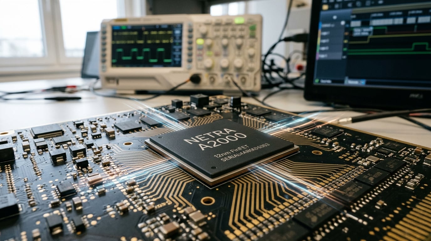
In the quest for technological self-reliance, the unveiling of the NETRA A2000 stands out as a watershed moment for India’s domestic deep-tech ecosystem. Developed by Kochi-based fabless semiconductor startup Netrasemi and nurtured under the Ministry of Electronics and Information Technology’s (MeitY) ambitious Design Linked Incentive (DLI) Scheme, the NETRA A2000 is officially recognized as India’s first indigenous Edge AI System-on-Chip (SoC).
During his interaction with 23 semiconductor chip design companies, Union Minister Shri Ashwini Vaishnaw highlighted the successful tape-out and design validation of this chip as a concrete proof-of-concept for the DLI scheme. Historically, Indian chip designers have acted as the back-end workforce for global silicon giants, performing physical design and verification. The NETRA A2000 shifts this dynamic entirely: it represents domestic ownership of high-value intellectual property (IP), designed in India, for both local and global markets.
Decoding the Tech: The 12nm Node and Edge AI Architecture
To understand the significance of the NETRA A2000, one must look at its architectural foundation and fabrication geometry. The SoC is designed on an advanced 12nm (nanometer) process node. In the semiconductor world, a smaller node size allows for a higher density of transistors, which translates directly to greater computational efficiency, lower power consumption, and a smaller physical footprint.
By choosing the 12nm node, Netrasemi has hit a highly competitive "sweet spot" for Edge AI applications:
- Energy Efficiency: Edge devices typically operate under strict thermal and power envelopes. The 12nm process enables the NETRA A2000 to execute complex machine learning algorithms locally without draining batteries or requiring bulky cooling systems.
- Low Latency: Traditional AI relies on sending raw data to centralized cloud servers for processing, which introduces latency and security vulnerabilities. As an Edge AI chip, the NETRA A2000 processes data directly on the device, dropping latency down to milliseconds.
- On-Chip Neural Processing: The SoC features dedicated neural processing hardware optimized for matrix multiplication and deep learning operations, allowing it to run convolutional neural networks (CNNs) and transformer models at the edge with remarkable speed.
Key Commercial Applications: Powering the Smart Vision Revolution
Union Minister Ashwini Vaishnaw emphasized that once the NETRA A2000 is deployed at a commercial scale, it will serve as the intelligence engine behind a myriad of smart vision and IoT devices. The target sectors for this chip are vast and rapidly expanding:
- Surveillance and Smart Cities: Real-time edge video analytics are critical for modern security frameworks. Devices powered by the NETRA A2000 can perform facial recognition, object detection, crowd anomaly detection, and license plate reading directly within the camera housing, eliminating the need to stream high-bandwidth, high-definition video feeds to centralized servers.
- Automotive and Mobility: The automotive industry is transitioning toward advanced driver assistance systems (ADAS). The NETRA A2000 can power in-cabin driver monitoring systems (detecting fatigue or distraction), lane-keep assist systems, and pedestrian detection algorithms, making active safety features more affordable and widely accessible in mid-range vehicles.
- Industrial IoT (IIoT) and Robotics: In automated factories, machine vision is used for high-speed quality inspections and robotic guidance. The NETRA A2000 can process visual feeds on the factory floor to identify manufacturing defects in real-time, preventing assembly line halts and reducing waste.
- Smart Consumer Electronics: From smart doorbells to advanced home automated systems, the chip can localise voice and gesture recognition, ensuring privacy-safe smart home environments where personal data never leaves the premises.
The Symbiosis of Indigenous Hardware and Advanced Software Platforms
The arrival of indigenous hardware like the NETRA A2000 signals a major leap forward, but hardware only achieves its full potential when paired with an equally sophisticated software and communication ecosystem. As edge devices become capable of processing complex video and sensory data locally, they will inevitably need to communicate downstream decisions, alerts, or queries to users and enterprise systems.
For instance, a smart surveillance camera powered by the NETRA A2000 might identify a critical safety breach on an industrial site. To act on this insight instantly, the edge device must trigger an automated, intelligent communication workflow. This is where advanced software infrastructures come into play. Platforms like CallMissed complement local hardware breakthroughs by offering enterprise-grade AI communication infrastructure.
+----------------------------------------+
|      Edge Layer: NETRA A2000 SoC       |
|  - Real-time video analytics           |
|  - Localized anomaly detection         |
+-------------------+--------------------+
                    | (Triggers Alert)
                    v
+----------------------------------------+
|  Cloud/API Layer: CallMissed Platform  |
|  - Multilingual TTS / STT (22 Langs)   |
|  - Low-latency Voice & SMS Alerts      |
+----------------------------------------+
By leveraging cloud-based LLM inference (with access to over 300+ models) and real-time Speech-to-Text and Text-to-Speech APIs that natively support 22 regional Indian languages, CallMissed can seamlessly turn edge-computed data into actionable, automated voice or WhatsApp interactions. A hybrid deployment where an edge-computing smart vision chip triggers a localized, multilingual voice agent via CallMissed could revolutionize remote asset monitoring, disaster management, and interactive customer kiosks across India's diverse linguistic landscape.
How the DLI Scheme Catalyzed this Breakthrough
The realization of the NETRA A2000 would have been highly improbable without the structured support of the Indian Government’s Design Linked Incentive (DLI) Scheme. Administered as part of the ₹76,000 crore India Semiconductor Mission (ISM), the DLI scheme provides financial incentives, design infrastructure support, and deployment assistance to domestic startups and MSMEs.
The DLI scheme’s multi-layered approach addresses the primary barriers to entry for fabless startup companies:
- Financial Risk Mitigation: Chip design is an incredibly capital-intensive endeavor with long gestation periods. DLI offers financial support of up to 50% of eligible expenditure, giving startups the financial runway needed to complete multiple design and simulation cycles.
- Access to EDA Tools: Through the scheme, MeitY has supported over 240 educational institutions and several design startups with access to world-class Electronic Design Automation (EDA) tools, IP cores, and prototyping facilities. This democratizes access to expensive software that would otherwise be cost-prohibitive for young firms.
- Facilitating Tape-outs: The physical manufacturing of the first prototype (the tape-out phase) is the most expensive hurdle in chip design. The DLI scheme actively supports startups during this high-risk phase, lowering the barriers to turning a digital schematic into physical silicon.
The success of Netrasemi's NETRA A2000 validates the strategic design of the DLI scheme. It proves that India is no longer just a destination for assembly and testing, but a viable hub for cutting-edge architectural design capable of competing on the global stage.
Scaling the Talent Pipeline: 240+ Academic Institutions Equipped

The global semiconductor race is fundamentally a talent race. While billions of dollars are poured into constructing state-of-the-art fabrication facilities (fabs) and assembly testing plants, the hardware is only as good as the architecture etched onto it. During his recent interaction with the Design Linked Incentive (DLI) scheme-approved startups, Union Minister Shri Ashwini Vaishnaw highlighted a foundational pillar of India’s semiconductor strategy: equipping over 240 academic institutions across the country with world-class chip design tools.
By bringing industry-standard tools directly to classrooms and research labs, the government is systematically addressing the talent deficit that has historically constrained the domestic VLSI (Very Large Scale Integration) sector. This massive educational enablement ensures that India transitions from a country of back-end verification engineers to a global powerhouse of front-end chip architects.
The Core Bottleneck: Demystifying EDA Tool Access
Historically, the highest barrier to entry for aspiring chip designers in India has not been raw intellectual capacity, but the prohibitive cost of Electronic Design Automation (EDA) tools. Software suites from global giants such as Synopsys, Cadence, and Siemens EDA are the lifelines of modern semiconductor engineering. Without them, designing, simulating, and verifying a complex System-on-Chip (SoC) is impossible.
A single commercial EDA license can cost tens of thousands of dollars annually per seat, a price point completely out of reach for the vast majority of Indian engineering colleges. Consequently, semiconductor education in Tier-2 and Tier-3 institutions was long restricted to theoretical textbooks or outdated, open-source simulators that failed to replicate real-world design constraints.
By equipping 240+ academic institutions with licensed, state-of-the-art EDA tools, the Ministry of Electronics and Information Technology (MeitY) has effectively democratized chip design.
- Leveling the Playing Field: Students at regional engineering colleges now have access to the exact same software suites used by silicon giants in Silicon Valley, Bengaluru, and Hsinchu.
- Hands-on Verification: Students can perform physical design, static timing analysis, and formal verification on actual advanced nodes, bridging the massive gap between academic theory and commercial tape-out readiness.
- Faculty Empowerment: Faculty members can now undertake cutting-edge research projects, collaborate with global semiconductor consortia, and publish high-impact papers based on real silicon design workflows.
Centralized Infrastructure: The Role of C-DAC and Central Portals
To manage the massive deployment of these highly sensitive and expensive software licenses, the Indian government has leveraged a centralized cloud-based delivery model. Under the aegis of the Centre for Development of Advanced Computing (C-DAC), academic institutions access EDA tools via secure, centralized servers. This "EDA-as-a-Service" model eliminates the need for individual colleges to invest in expensive local high-performance computing (HPC) clusters, which are notorious for high maintenance costs and rapid obsolescence.
Through this centralized pipeline, students can design their chips locally and upload their GDSII (Graphic Database System II) files directly to central repositories. This infrastructure directly feeds into the government’s broader goal of supporting "Chips to Startup" (C2S) program, which aims to train 85,000 highly skilled engineers in VLSI and embedded system design over a five-year period.
Fostering Industry-Ready VLSI Engineers
The integration of 240+ academic institutions into the semiconductor design fold addresses a critical pain point for domestic design startups. Historically, Indian startups under the DLI scheme struggled to recruit local talent that understood modern, sub-28nm design rules. Most fresh graduates required six to twelve months of intensive corporate retraining before they could contribute to a live project.
Now, with students graduating with hands-on experience in physical design, DFT (Design for Testability), and analog layout:
- Onboarding Cycles are Slashed: Startups can hire "plug-and-play" engineers who can immediately navigate complex design partitions.
- Encouraging Entrepreneurship: Armed with design tool proficiency, academic researchers are spinning out their own fabless startups directly from university incubation cells.
- Optimizing Lower Nodes: Training students on advanced nodes (such as 28nm, 12nm, and below) prepares them for the next wave of high-performance computing, automotive electronics, and 5G/6G communication chips.
Fueling the Edge AI and Telecom Revolution
The downstream impact of this talent pipeline is already visible in the commercial breakthroughs achieved under the DLI scheme. For example, Netrasemi’s development of the NETRA A2000—India’s first Edge AI System-on-Chip designed on an advanced 12nm node—highlights the complex computational problems domestic designers are tackling. Building such sophisticated edge AI processors requires engineers who intimately understand neural network acceleration, low-power physical design, and thermal management.
As the talent pipeline scales, these specialized skills will become critical across the broader technology ecosystem. For instance, advanced communication architectures depend heavily on optimized silicon to process massive amounts of voice and data with ultra-low latency.
In this landscape, platforms like CallMissed—which provide advanced AI communication infrastructure, including voice agents, LLM inference, and multi-model API gateways—stand to benefit immensely. While CallMissed enables businesses to deploy production-ready AI voice agents seamlessly, the underlying performance of these real-time LLM inference models is ultimately bounded by hardware efficiency. As India-trained engineers design custom, low-cost edge AI and telecom chips, companies like CallMissed can look forward to deploying hyper-localized, ultra-low latency Speech-to-Text and voice synthesis models directly on cost-effective, domestic hardware. Furthermore, with platforms like CallMissed building multilingual AI agents supporting 22 regional Indian languages, having local chip designers optimize silicon architecture for Indic natural language processing (NLP) will create a self-sustaining cycle of hardware-software co-design.
Bridging Academic Design with Commercial Deployment
The ultimate goal of equipping these 240+ institutions is to create a seamless pipeline where a student project can mature into a commercial startup. By integrating university labs with the DLI scheme, the government has established a clear roadmap:
[Academic Labs (EDA Tools)] ➔ [C2S Program / IP Creation] ➔ [DLI Scheme Funding] ➔ [Commercial Tape-Out & Fabs]This structural link ensures that intellectual property (IP) created in Indian classrooms does not remain locked in academic archives. Instead, it is actively nurtured, funded under the DLI scheme, and channeled toward fabrication. Shri Ashwini Vaishnaw’s engagement with these startups underscores the government's commitment to ensuring that the brilliant designs originating in these 240+ newly equipped classrooms find their way onto actual silicon wafers, positioning India as a global epicentre for end-to-end semiconductor innovation.
Comparative Analysis: India's DLI Scheme vs Global Semiconductor Incentives
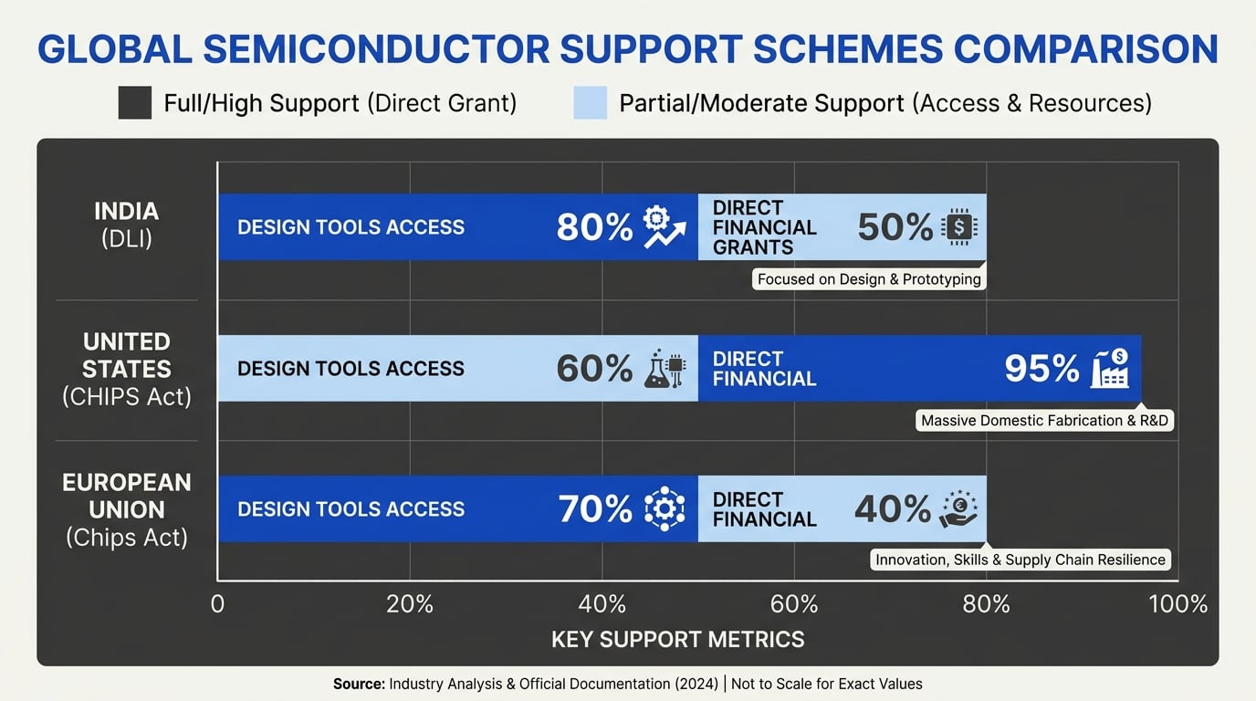
The global semiconductor race has transformed from a corporate competition into a high-stakes geopolitical battlefield. As countries vie for technological sovereignty, governments worldwide are deploying massive fiscal bazookas to attract silicon manufacturing and design talent.
When Union Minister Shri Ashwini Vaishnaw met with 23 semiconductor chip design companies under the Design Linked Incentive (DLI) scheme, the discussion highlighted a distinct paradigm. While economic giants like the United States, the European Union, and East Asian nations focus heavily on multi-billion-dollar physical fabrication plants (fabs), India is pioneering a highly targeted, intellectually intensive path. By analyzing India's DLI scheme against global semiconductor policies, we can better understand the unique strengths, challenges, and strategic direction of India's silicon ambitions.
The Architecture of India’s DLI Scheme: A Focus on IP
The DLI scheme, managed under the India Semiconductor Mission (ISM), represents a departure from traditional industrial subsidies. Instead of merely funding brick-and-mortar facilities, the DLI targets the high-value, intellectual-property-heavy segment of the semiconductor value chain: chip design.
The scheme offers two primary financial pillars to domestic startups, MSMEs, and research institutions:
- Design Infrastructure Support: Up to 50% of the eligible expenditure (capped at ₹15 Crore per application) is reimbursed for design development, alongside access to world-class Electronic Design Automation (EDA) tools, IP cores, and prototyping systems.
- Product Deployment Linked Incentive: An incentive of 4% to 6% of net sales turnover over five years (capped at ₹30 Crore per application) is awarded for successfully deploying designed chips in commercial products.
This strategic focus has already yielded tangible breakthroughs. A prime example is Netrasemi, which designed India's first Edge AI System-on-Chip (SoC)—the NETRA A2000—on an advanced 12nm node. When deployed commercially, this chip will power smart vision applications in surveillance, automotive systems, and consumer electronics. Additionally, by extending world-class EDA design tools to 240 educational institutions, the Indian government is systematically building a continuous pipeline of VLSI (Very Large Scale Integration) design engineers.
How India’s DLI Compares to Global Initiatives
To appreciate the distinct nature of the DLI scheme, it is helpful to contrast it with the massive capital-intensive frameworks deployed by other global powers.
| Region / Scheme | Primary Focus | Financial Commitments | Key Targets |
|---|---|---|---|
| India (DLI Scheme) | Fabless Chip Design, IP Creation, and Local Startups | $10 Billion (Overall ISM budget, with targeted DLI caps) | Startups, MSMEs, and academic talent pipeline |
| United States (CHIPS Act) | Onshoring Leading-Edge Manufacturing (Fabs) & R&D | $52.7 Billion in direct funding and loans | Mega-fabs (TSMC, Intel, Samsung) and packaging plants |
| European Union (EU Chips Act) | Doubling Global Manufacturing Share & Advanced Design | €43 Billion in public and private investments | Megafabs, pilot lines, and pan-European research |
| South Korea (K-Chips Act) | Retaining Dominance in Memory & Logic Manufacturing | Up to 30%-50% Tax Credits for R&D and facilities | Domestic giants (Samsung, SK Hynix) |
#### 1. India vs. The US CHIPS and Science Act
The US CHIPS Act is designed to mitigate supply chain vulnerabilities by physically moving advanced manufacturing back to American soil. It is heavily capital-intensive, distributing tens of billions of dollars to giants like Intel, TSMC, and Samsung to construct multi-billion-dollar fabs in Arizona, Ohio, and Texas.
In contrast, India's DLI scheme targets the "fabless" startup model. Fabless companies design the chips but outsource the actual manufacturing to global foundries. By focusing on design rather than immediate leading-edge fabrication, India avoids the astronomical, recurring capital expenditures of modern 3nm or 2nm fabs. Instead, India captures high-value intellectual property, which yields higher profit margins and long-term asset value.
#### 2. India vs. The EU Chips Act
The European Union's €43 billion initiative seeks to double its global semiconductor market share to 20%. While the EU Chips Act includes a "Chips for Europe" initiative to support design, the bulk of its momentum is aimed at setting up mega-fabs (such as Intel’s planned facilities in Germany) and establishing advanced pilot lines.
India's approach is more decentralized and agile. Rather than trying to match the sheer financial scale of European subsidies, India focuses on local design customization—building specific application SoCs for telecom, smart energy meters, IoT, and edge-intelligence devices tailored to emerging market requirements.
#### 3. India vs. East Asian Incentives (South Korea & Taiwan)
South Korea’s K-Chips Act and Taiwan’s established industrial policies rely heavily on massive tax credits and infrastructure guarantees for domestic conglomerates like TSMC, Samsung, and SK Hynix. These nations are focused on maintaining their absolute global dominance in advanced manufacturing and high-bandwidth memory (HBM).
India’s DLI, conversely, is explicitly democratized. By capping individual project incentives and directing resources toward MSMEs and academia, the policy fosters an ecosystem of diverse, agile startups rather than consolidating wealth into a few mega-corporations.
The Synergy Between Silicon and Software
The true success of India's DLI scheme will not be measured solely by the number of chips designed, but by how effectively those chips integrate into the broader digital and software ecosystem. The rise of local Edge AI chips like the NETRA A2000 is highly complementary to India’s booming AI software and infrastructure sector.
For example, next-generation AI communication platforms like CallMissed rely heavily on specialized hardware to execute complex, low-latency tasks. Platforms like CallMissed—which orchestrates advanced voice agents, LLM inference across over 300 models, and real-time Speech-to-Text APIs supporting 22 regional Indian languages—benefit immensely when the underlying silicon is optimized for Edge AI. As Indian startups design chips tailored for localized natural language processing and computer vision, software platforms can run complex conversational AI algorithms with reduced latency, lower power consumption, and enhanced data privacy.
Key Advantages and Strategic Outlook
India’s DLI scheme offers several unique advantages that position the country well in the global semiconductor landscape:
- Capital Efficiency: By focusing on design, India leverages its strongest asset—its massive pool of software and VLSI engineering talent—without requiring the immediate, massive capital investments needed for advanced lithography manufacturing.
- National Security & Sovereignty: Designing indigenous SoCs for critical sectors like telecom, defense, and power grids ensures that the core instruction set architectures and hardware Trojan protections remain entirely within domestic control.
- Talent Democratization: Supplying EDA tools to 240 universities ensures that the next generation of engineers enters the workforce with hands-on, practical experience in advanced node design.
While the US, EU, and East Asia continue their high-stakes capital war over physical fabrication plants, India's DLI scheme is quietly laying the groundwork for a formidable, intellectually independent fabless ecosystem. By fostering high-value IP creation locally, India is positioning itself not just as a manufacturing destination, but as the brain trust of the global semiconductor future.
Impact & Implications: From Design to Commercial Scale
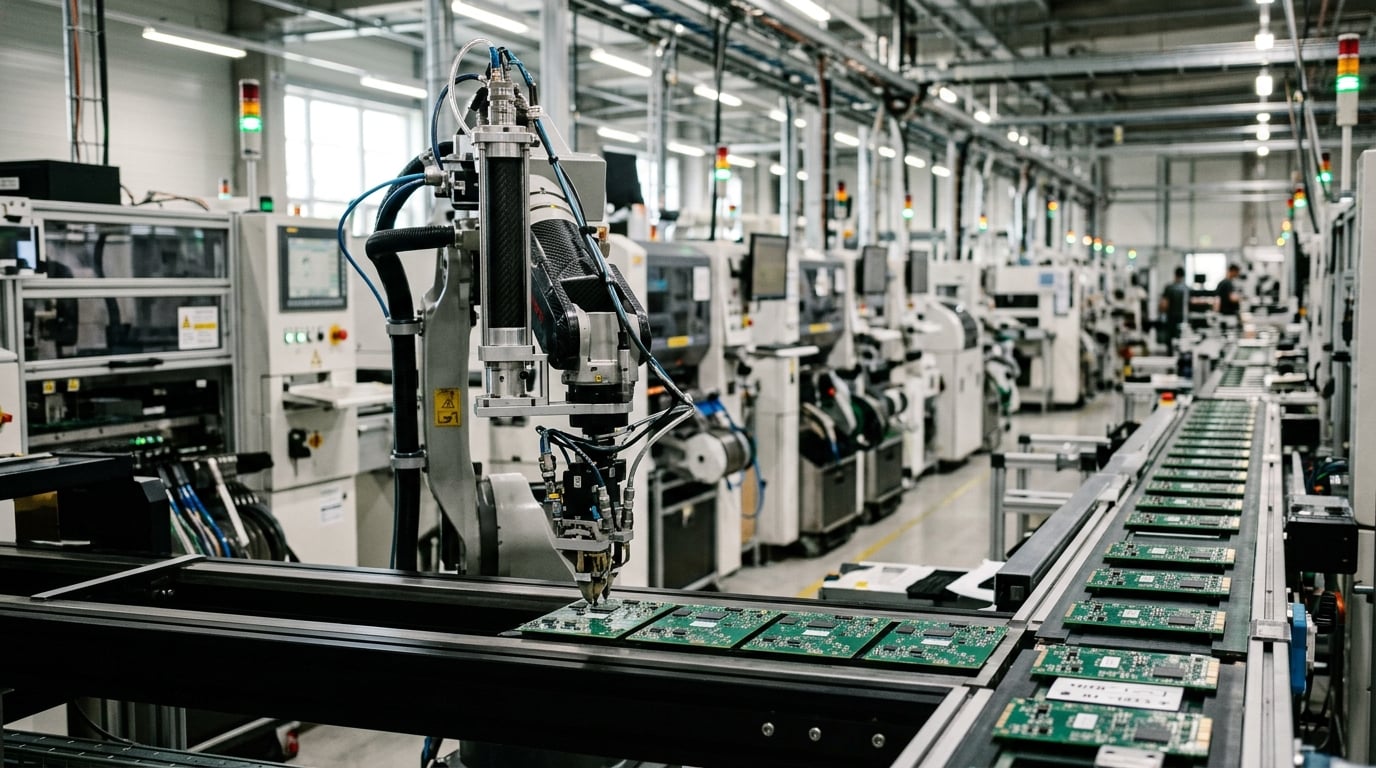
The transition of India’s semiconductor strategy from theoretical blueprinting to tangible, commercial-scale silicon represents a massive paradigm shift for the nation's technology ecosystem. For years, India has been recognized as a powerhouse for backend chip design talent, hosting design centers for almost all of the world's top semiconductor giants. However, the domestic ownership of intellectual property (IP) remained minimal.
With the Design Linked Incentive (DLI) scheme showing early, concrete successes, the conversation has officially shifted. During his interaction with semiconductor chip design companies, Union Minister for Electronics and Information Technology Shri Ashwini Vaishnaw highlighted how domestic design firms are successfully moving down the commercialization pipeline. The implications of this transition extend far beyond the laboratory, directly influencing sectors ranging from defense and automotive to consumer electronics and telecommunications.
From Blueprints to Silicon: The Edge AI Revolution
The most prominent example of the DLI scheme’s real-world impact is the development of the NETRA A2000 by Indian chip design startup Netrasemi. As India’s first domestic Edge AI System-on-Chip (SoC) built on an advanced 12nm node, the NETRA A2000 is a prime demonstration of high-performance, low-power hardware designed to meet localized computing demands.
Moving computing tasks from centralized cloud data centers to the "edge"—directly on the physical device—requires highly specialized chip architecture. The commercial deployment of the NETRA A2000 is poised to catalyze several critical industries:
- Smart Vision & Surveillance: Local processing of video feeds allows for real-time threat detection, facial recognition, and spatial analysis without the latency or bandwidth costs of uploading video streams to the cloud.
- Automotive Systems: Advanced Driver Assistance Systems (ADAS) require split-second decision-making. Edge AI chips process sensor and camera feeds locally, ensuring the ultra-low latency necessary for autonomous braking and collision avoidance.
- Industrial IoT: Factories can deploy intelligent sensors that predict machine failures locally, saving millions in potential downtime.
By taking a 12nm chip from design to physical silicon, domestic firms are proving that they can navigate the complex global supply chain, coordinate with international fabrication plants (foundries), and deliver market-ready hardware.
Synergizing Hardware Breakthroughs with Intelligent Software
The arrival of domestic Edge AI chips creates a powerful feedback loop with software developers. Hardware alone cannot drive commercial transformation; it requires a robust, integrated software layer to translate processing power into enterprise value. As local chips lower the hardware cost of AI inference, software platforms must evolve to support these edge deployments.
For example, platforms like CallMissed are already building the communications infrastructure that can leverage high-performance local and hybrid processing capabilities. While CallMissed provides enterprise-grade AI communication tools—including low-latency voice agents, LLM inference across 300+ models, and advanced Speech-to-Text APIs supporting 22 regional Indian languages—the long-term synergy with domestic hardware like the NETRA A2000 is clear.
As Indian enterprises deploy localized hardware in remote, edge-based systems, having software solutions capable of processing complex, multilingual communications natively on the edge will unlock unprecedented operational efficiency. This combination of domestic silicon and localized, multi-model AI platforms ensures that Indian businesses can deploy secure, low-latency, and highly contextual communication frameworks without relying entirely on foreign cloud infrastructure.
Building the Academic and Human Capital Foundation
Scaling chip design to a commercial level is impossible without a continuous pipeline of highly skilled engineers. Recognizing this bottleneck, the Indian government has paired the DLI scheme with a massive educational push, equipping 240 academic and educational institutions across the country with world-class, industry-standard chip design tools.
This educational integration ensures that the next generation of engineers is trained on the exact software, electronic design automation (EDA) tools, and methodologies used by modern semiconductor firms. Key benefits of this talent-pipeline initiative include:
- Reduced Onboarding Times: Engineering graduates can transition immediately into active R&D roles within the 23 approved DLI companies and other global design houses without requiring months of remedial training.
- Democratized Access to EDA Tools: Historically, EDA software licenses from industry giants were prohibitively expensive for local universities. Government-backed access levels the playing field for students from tier-2 and tier-3 institutions.
- Encouraging Grassroots IP Creation: Armed with professional-grade design tools, university research labs can incubate their own micro-architectures, feeding new IPs directly into the national ecosystem.
Economic Autonomy and Global Competitive Advantage
The commercialization of domestic designs directly addresses India’s strategic vulnerability regarding semiconductor imports. By transitioning from a consumer of global silicon to a creator of proprietary chip architectures, India secures several economic and strategic advantages:
- Customized Solutions for the Global South: Indian design firms are uniquely positioned to build highly optimized, cost-effective SoCs tailored for emerging markets. These markets require ruggedized, low-power hardware that can operate reliably under erratic power supplies and in varying environmental conditions.
- Mitigation of Supply Chain Shocks: Having domestically owned chip designs allows Indian manufacturers to negotiate more flexibly with global foundries, ensuring that domestic industries—such as telecom and automotive—are less vulnerable to sudden geopolitical tensions or global fab closures.
- Capture of High-Value IP Margins: In the semiconductor value chain, the largest profit margins belong to the companies that own the IP, not necessarily the foundries that manufacture them. By shifting from contract testing and packaging to IP ownership, Indian companies can capture a far greater share of the global semiconductor market's economic value.
With 24 projects already approved under the DLI scheme, India is demonstrating that it has the technical capability, government backing, and academic infrastructure required to transition chips from a digital layout file to high-volume physical production. This marks the beginning of an era where Indian-designed, Indian-owned silicon will power global technologies.
Expert Opinions & Policy Outlook
The Strategic Paradigm Shift: From Backend Support to Global IP Ownership
Industry analysts and semiconductor experts view Union Minister Shri Ashwini Vaishnaw’s recent high-level interaction with 23 chip design companies as a watershed moment for India's technology ecosystem. For decades, India has been a powerhouse for global semiconductor engineering, hosting design centers for almost all major global chipmakers. However, the intellectual property (IP) and profits generated by these engineers historically remained with overseas multinationals.
The Design Linked Incentive (DLI) Scheme represents a structural shift in this dynamic. By focusing policy support directly on domestic startups and MSMEs, the government is deliberately pivoting from an ecosystem of outsourced engineering services to one of domestic IP ownership. Industry experts point out that owning the underlying chip design is where the highest value lies in the global semiconductor value chain. With 24 projects already approved under the scheme, India is transitioning from a service-driven technology exporter to a product-driven semiconductor hub.
The policy outlook indicates that the government intends to double down on these initial successes. By funding up to 50% of eligible expenditure and providing design infrastructure support, the DLI scheme acts as a crucial safety net for high-risk, high-capital hardware startups, encouraging local entrepreneurs to design complex System-on-Chips (SoCs), application-specific integrated circuits (ASICs), and telecom microprocessors directly on Indian soil.
Deconstructing Netrasemi’s NETRA A2000: A Milestone in Edge AI
Among the major success stories highlighted during the Minister’s interactive session was Netrasemi, an Indian fabless semiconductor company that has successfully designed the NETRA A2000. This chip stands out as India’s first domestically designed Edge AI System-on-Chip (SoC) fabricated on an advanced 12nm node.
Technical analysts emphasize that the 12nm node represents a highly sophisticated and commercially viable technology tier. The development of the NETRA A2000 offers several key advantages for the domestic and global markets:
- Low Latency Edge Processing: By processing artificial intelligence workloads directly on-device (at the "edge") rather than sending data back and forth to a distant cloud server, the chip slashes latency and bandwidth requirements.
- Commercial Applications: The chip is optimized to power smart vision applications across high-growth sectors, including smart surveillance, autonomous automobiles, and advanced industrial automation.
- Sovereign Data Privacy: Edge processing inherently keeps sensitive data on-site, a critical requirement for national security, defense, and localized enterprise deployments.
Experts agree that the commercial deployment of the NETRA A2000 will serve as a powerful proof of concept for the DLI scheme, signaling to international venture capitalists that Indian startups can execute complex, tape-out ready silicon designs.
Fostering a Sustained Talent Pipeline: The 240 Institutions Initiative
One of the most praised aspects of India's current semiconductor policy is its focus on long-term sustainability. During the interaction, Minister Vaishnaw highlighted that the government has supported 240 educational institutions across the country with world-class chip design tools.
Historically, accessing Electronic Design Automation (EDA) tools from global giants was prohibitively expensive for Indian universities, restricting hands-on chip design education to a tiny fraction of elite institutions. By democratizing access to these specialized software suites, the government is actively training a massive cohort of "tape-out ready" engineers.
Educational experts believe this policy will yield a highly competitive demographic dividend. Within the next few years, India is projected to produce tens of thousands of skilled VLSI (Very Large Scale Integration) engineers annually. This vast talent pool will not only feed domestic startups but will also make India an irresistible destination for global semiconductor firms looking to establish joint research and development centers.
The Symbiosis of Sovereign Silicon and Advanced Software Systems
The emergence of domestic hardware like the NETRA A2000 has direct, positive ramifications for India's booming software and artificial intelligence sectors. High-performance, locally designed AI silicon enables software developers to build applications optimized specifically for local infrastructure constraints, such as variable power grids and localized language processing.
As next-generation AI agents and speech interfaces scale across the country, having optimized edge hardware becomes critical. For example, modern AI communication platforms require immense processing power to handle complex voice and language translation workloads. Infrastructure platforms like CallMissed rely heavily on fast, low-latency processing to power their real-time voice agents, Speech-to-Text APIs supporting 22 regional Indian languages, and multi-model LLM routing.
When domestic hardware architectures like the NETRA A2000 are deployed at scale, software engines and communication infrastructures can run voice and data workloads locally, dramatically lowering operational costs and latency. This synergy between sovereign chip design and advanced software infrastructure platforms like CallMissed will be key to unlocking mass-market AI tools that can interact naturally in regional dialects without relying on expensive, cloud-hosted foreign servers.
Policy Outlook: The Path to India's Semiconductor Sovereignty
Looking ahead, policy analysts expect a continued convergence of the DLI scheme with other pillars of the India Semiconductor Mission (ISM), such as the assembly, testing, marking, and packaging (ATMP) and wafer fabrication incentives. The ultimate goal is to build a completely self-sustaining, vertically integrated semiconductor ecosystem within the country.
Key trends shaping the policy outlook over the next few years include:
- Increased Funding Allocation: Given the encouraging early results, industry bodies are advocating for an expansion of the DLI budget to support a broader array of niche chip architectures, such as power electronics and RF (Radio Frequency) chips.
- Focus on Local Fab Integration: As domestic fabs and assembly units come online in states like Gujarat and Assam, the government will likely incentivize DLI-approved startups to manufacture their designed chips locally, creating a closed-loop domestic supply chain.
- Government Procurement Mandates: Analysts predict that future policy updates may introduce preferential market access (PMA) guidelines, encouraging government departments and public sector undertakings to prioritize equipment powered by "designed-in-India" silicon.
Through targeted financial incentives, comprehensive talent development at 240 academic institutions, and a clear focus on high-value IP creation, the Indian government's semiconductor strategy is successfully laying the groundwork for long-term technology leadership on the global stage.
What This Means For You
The rapid acceleration of India’s semiconductor ecosystem under the Design Linked Incentive (DLI) Scheme is more than just a macroeconomic milestone—it is a foundational shift that directly impacts developers, startups, enterprises, and the broader technology landscape. By providing crucial financial incentives and design infrastructure support, the Ministry of Electronics and Information Technology (MeitY) is actively lowering the barrier to entry for domestic hardware innovation.
For businesses and innovators, this initiative bridges the gap between raw software capabilities and localized hardware execution. As domestic fabless startups successfully design cutting-edge silicon, enterprises gain access to highly optimized, cost-effective, and secure hardware tailored for Indian deployment conditions.
The table below outlines how these policy-driven developments translate into tangible benefits across different segments of the technology ecosystem:
| Stakeholder Group | Key DLI Development | Direct Opportunity | Core Target Sectors |
|---|---|---|---|
| Startups & Fabless Firms | Financial incentives, EDA tool access, and design support | Faster prototyping and reduced time-to-market for custom ASICs/SoCs | IoT, Telecom, Automotive, Edge AI |
| Enterprises & OEMs | Local sourcing of indigenously designed chips (e.g., NETRA A2000) | Reduced import dependency, lower bill-of-materials (BOM), and secure supply chains | Smart Cities, Surveillance, Logistics |
| Software & AI Developers | Hardware-software co-design and optimized Edge silicon | Ultra-low-latency deployment of localized LLMs and Speech-to-Text models | Conversational AI, Robotics, Industrial Automation |
| Academia & Researchers | Access to world-class chip design tools in 240 institutions | Hands-on training on modern VLSI design and advanced nodes (up to 12nm) | Deep-tech R&D, Defence, Aerospace |
1. Accelerated Edge AI and Smart Applications
One of the most significant breakthroughs highlighted by Union Minister Shri Ashwini Vaishnaw is the commercial viability of domestic Edge AI systems. Indian fabless pioneer Netrasemi has successfully designed the NETRA A2000, India’s first indigenously designed Edge AI System-on-Chip (SoC) built on an advanced 12nm node.
For developers and system integrators, this represents a massive leap forward:
- Smart Vision & Surveillance: Localized processing allows security and smart city cameras to execute real-time video analytics, facial recognition, and anomaly detection directly on the device, eliminating expensive cloud bandwidth costs.
- Automotive & IoT: Automotive OEMs can integrate ultra-low-latency driver monitoring systems and advanced driver-assistance systems (ADAS) powered by domestic silicon.
- Data Privacy: Because data is processed at the edge, sensitive enterprise and consumer information does not need to leave the local network, ensuring compliance with strict data protection frameworks.
2. Democratization of Chip Design & Talent Pool
Historically, chip design was restricted to massive multinational corporations due to the prohibitive cost of Electronic Design Automation (EDA) tools and licensing. The DLI scheme is systematically dismantling these barriers. By equipping 240 educational institutions across India with world-class chip design software, the government is cultivating a highly skilled, industry-ready VLSI (Very Large Scale Integration) workforce.
This means tech companies looking to build hardware-dependent solutions will soon have access to a massive talent pool capable of custom silicon engineering. Startups no longer need to rely entirely on off-the-shelf, generalized processors; they can design application-specific integrated circuits (ASICs) optimized precisely for their software workloads.
3. Native Integration: Hardware Meets AI Software
The convergence of domestic silicon and advanced software platforms creates unprecedented opportunities for communication and automation. High-performance Edge AI chips require robust software pipelines to deliver real-world value.
This is where advanced communication infrastructure platforms like CallMissed step in. As local hardware handles heavy localized computing workloads, platforms like CallMissed can seamlessly orchestrate the cloud-to-edge software layer. For instance, developers can combine localized Edge AI processors with CallMissed's specialized APIs—which support Speech-to-Text across 22 Indian languages—to deploy highly responsive, multilingual voice agents and WhatsApp chatbots.
By running optimized, local speech-processing models on domestic chips while relying on CallMissed’s multi-model API gateway (supporting 300+ LLMs), enterprises can achieve:
- Sub-second Latency: Crucial for natural, real-time voice conversations.
- Offline Resilience: The ability to handle basic automated voice sorting and localized data logging even during temporary internet outages.
- Hyper-Localization: Delivering voice experiences that accurately understand regional accents and dialects across India’s diverse demographics.
Ultimately, the DLI scheme ensures that the future of Indian technology is built on a self-reliant foundation—where domestic silicon and state-of-the-art AI communication platforms work in tandem to power the next generation of enterprise automation.
The Road Ahead: Building a Sovereign Silicon Ecosystem

The realization of an Atmanirbhar Bharat (self-reliant India) in the technology sector hinges on a critical pivot: transitioning from being a consumer of global technology to becoming a primary creator of intellectual property (IP). As Union Minister for Electronics and Information Technology Shri Ashwini Vaishnaw emphasized during his historic interaction with domestic semiconductor design leaders, the ultimate goal of the Design Linked Incentive (DLI) Scheme is to establish a robust, sovereign silicon ecosystem.
Building this sovereign ecosystem requires a multi-pronged approach that goes beyond merely manufacturing chips. It demands domestic ownership of the fundamental designs, a continuous pipeline of highly skilled VLSI (Very Large Scale Integration) engineers, and a thriving commercial market eager to adopt homegrown silicon.
The Strategic Blueprint of the DLI Scheme
For decades, India has been the back-office brain for global semiconductor giants, hosting a massive portion of the world's chip design talent. However, the intellectual property designed on Indian soil historically belonged to foreign multinational corporations. The DLI Scheme directly addresses this gap by offering financial incentives, design infrastructure support, and deployment assistance to domestic startups and MSMEs.
By approving 24 projects and actively supporting 23 semiconductor chip design companies, the government is systematically fostering a local IP repository. The scheme targets critical, high-growth domains:
- System-on-Chips (SoCs): Integrating all necessary electronic circuits and parts onto a single microchip to power complex computing systems.
- Telecom Equipment Chips: Developing localized chipsets to secure India’s rapidly growing 5G and future 6G networks.
- Next-Generation IoT Devices: Creating power-efficient microcontrollers for smart infrastructure, agriculture, and industrial automation.
Netrasemi’s NETRA A2000: A Milestone in Sovereign Edge AI
The tangible impact of this sovereign design push is already visible. A prime example highlighted by Minister Vaishnaw is the success of the Indian semiconductor company Netrasemi. Under the DLI scheme, Netrasemi has successfully designed India's first Edge AI System-on-Chip (SoC)—the NETRA A2000—built on an advanced 12nm node.
Developing a chip on a 12nm node represents a major leap in domestic engineering capabilities. The NETRA A2000 is designed to run complex artificial intelligence algorithms directly on the device ("at the edge") rather than relying on distant, energy-hungry cloud data centers. When deployed at a commercial scale, this chip will power smart vision applications across several vital sectors:
- Surveillance and Public Safety: Enabling real-time, low-latency video analytics directly within security cameras.
- Automotive Systems: Powering advanced driver assistance systems (ADAS) and intelligent vehicle telemetry.
- Industrial IoT: Facilitating predictive maintenance and high-speed quality inspections in automated factories.
Cultivating the Talent Pipeline at the Grassroots
A sovereign silicon ecosystem cannot survive without a steady influx of world-class design talent. To ensure that Indian startups never face a shortage of skilled engineers, the government has launched a massive academic enablement initiative.
Under this program, the Ministry of Electronics and Information Technology (MeitY) has equipped 240 educational institutions across India with state-of-the-art, world-class chip design tools. Traditionally, access to professional Electronic Design Automation (EDA) software was prohibitively expensive for most Indian universities. By democratizing access to these industrial-grade tools, thousands of students are now graduating with hands-on experience in modern chip design, bridging the gap between academia and the semiconductor industry.
The Convergence of Sovereign Hardware and Localized Software
Developing local hardware is only half the battle; these chips must integrate seamlessly with software designed to solve local challenges. As India builds out its Edge AI silicon layer, the software ecosystem must evolve in parallel to unlock its full potential.
This is where advanced software platforms are matching the hardware revolution step-for-step. For instance, while chips like the NETRA A2000 process visual and cognitive data at the edge, AI communication platforms like CallMissed are building the sovereign software infrastructure to match. CallMissed provides businesses with conversational AI voice agents, LLM inference across over 300 models, and Speech-to-Text APIs that natively support 22 regional Indian languages.
When homegrown Edge AI chips are paired with localized software suites like CallMissed, businesses can deploy hyper-local, secure, and latency-free communication solutions. This hardware-software synergy ensures that data remains within national borders, boosting data sovereignty while driving down the operational costs of AI deployments.
Challenges on the Horizon: From Tape-Out to Mass Production
While the progress under the DLI Scheme is highly encouraging, the road ahead is not without obstacles. Designing a chip (achieving "tape-out") is an expensive milestone, but transitioning that design into high-volume commercial production requires navigating complex global supply chains.
- Fabrication Partnerships: Since India's commercial fabrication plants (fabs) are still under construction, domestic design firms must temporarily secure manufacturing slots with global foundries.
- Capital Intensity: Chip design is a capital-intensive journey with long gestation periods. Continuous funding rounds and government support are vital to keep startups afloat before they reach commercial viability.
- Market Adoption: Indian system integrators and original equipment manufacturers (OEMs) must actively prioritize domestic chips over established global alternatives to create a self-sustaining cycle of demand.
By fostering domestic IP creation, empowering academic institutions, and encouraging software-hardware integration, India is laying a rock-solid foundation for a resilient, self-sustaining silicon future. The progress celebrated by Minister Vaishnaw and the DLI-approved companies signals that India is no longer just a participant in the global digital economy—it is fast becoming one of its primary architects.
Frequently Asked Questions
As India accelerates its journey toward becoming a global semiconductor powerhouse, the Design Linked Incentive (DLI) Scheme under the India Semiconductor Mission (ISM) has emerged as a crucial pillar for fostering domestic innovation. The recent interactive session between Union Minister for Electronics and Information Technology, Shri Ashwini Vaishnaw, and key stakeholders from various semiconductor startups highlighted both the rapid progress of native silicon development and the government's strategic roadmap to address industry challenges. Below, we address some of the most pressing questions regarding this landmark initiative, its technological breakthroughs, and its broader implications for India's digital future.
What is the primary purpose of the interaction between Union Minister Shri Ashwini Vaishnaw and the semiconductor chip design companies approved under the DLI Scheme?
How does the Design Linked Incentive (DLI) Scheme financially and technically assist Indian semiconductor startups?
What major technological milestones have been achieved by semiconductor chip design companies approved under the DLI Scheme, such as Netrasemi?
How is the government addressing talent development and tool availability for semiconductor chip design companies approved under the DLI Scheme?
Which commercial industries stand to benefit the most from the silicon designs currently emerging from the DLI Scheme?
How do the hardware advancements driven by the DLI Scheme impact software platforms like AI-driven communication infrastructures?
The progress of the DLI Scheme marks a defining moment in India’s quest to transition from a digital consumer nation to a global technology creator. By actively supporting domestic chip design companies and building a vast talent pool across academic institutions, India is establishing a robust foundation for a self-sustaining technology stack. As advanced silicon designs move from fabrication to real-world integration, they will fuel a new wave of software innovation, enabling platforms like CallMissed to provide faster, more secure, and highly efficient AI communication tools that empower businesses worldwide.
Conclusion
The interaction between Union Minister Shri Ashwini Vaishnaw and local chip designers underscores a pivotal shift in India's technology ecosystem. No longer just a global hub for software talent, India is rapidly positioning itself as a dominant force in semiconductor intellectual property.
Key takeaways from this landmark phase of the DLI Scheme include:
- Pioneering Local Silicon: The success of homegrown designs like Netrasemi's NETRA A2000—India's first Edge AI System-on-Chip (SoC) designed on an advanced 12nm node—proves that domestic startups can innovate at the cutting edge.
- Nurturing the Talent Pipeline: By equipping 240 educational institutions with world-class chip design tools, the government is securing a highly skilled workforce to sustain long-term industry growth.
- Broad Industry Impact: With 24 projects approved, these domestic chips will soon power commercial smart vision applications, telecom infrastructure, and automotive systems nationwide.
Looking ahead, watch for India to accelerate its transition from a hardware importer to a primary exporter of proprietary semiconductor IP. As domestic silicon enters commercial production, it will fuel an explosive rise in localized Edge AI capabilities, bringing processing power closer to the user with unprecedented efficiency.
To explore how AI communication is evolving alongside this hardware revolution, check out CallMissed — an AI infrastructure platform powering voice agents and multilingual chatbots for businesses. As India's silicon and software ecosystems converge, how will your business leverage this next generation of intelligent, locally powered infrastructure?
Discussion
Related Posts



Ready to automate customer conversations?
Launch AI voice agents and WhatsApp bots with CallMissed — one API, 22+ Indian languages.