IBM Debuts World’s First Sub-1 Nanometer Chip Technology: The Future of Semiconductor Innovation
IBM Debuts World’s First Sub-1 Nanometer Chip Technology: The Future of Semiconductor Innovation
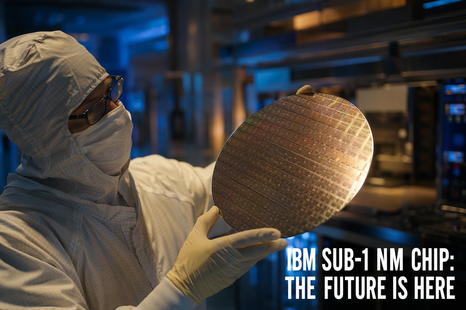
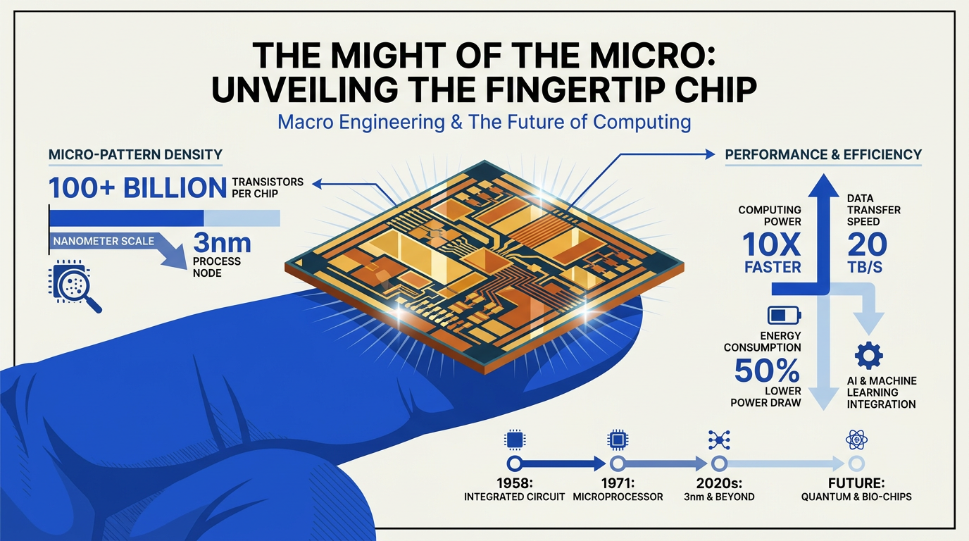
Imagine cramming nearly 100 billion transistors onto a chip the size of a fingernail—sounds like science fiction, yet it’s today’s reality. On June 25, 2026, IBM stunned the tech world by unveiling the world’s first sub-1 nanometer chip technology, a breakthrough destined to redefine the future of semiconductor innovation [1]. Powered by a revolutionary “nanostack” 3D architecture, this chip achieves almost twice the transistor density of IBM’s own 2 nm predecessor, promising performance gains of up to 50% and energy efficiency improvements exceeding 70% compared to previous generations [4]. In an era where demand for AI acceleration, cloud computing, and edge devices shows no sign of slowing—IDC forecasts global semiconductor revenues will top $1.2 trillion by 2030—IBM’s leap puts the industry on a new trajectory.
What makes this such a seismic shift? Shrinking chip features below the 1 nm threshold isn’t just a matter of miniaturization. It’s a materials and engineering marathon, rewriting what’s possible for everything from high-performance data centers to battery-powered IoT devices. With transistor scaling approaching its physical limits, IBM’s innovation rekindles Moore’s Law, extending advances in speed, power, and cost that underpin today’s digital economy. As the web of digital infrastructure grows—fueling applications like generative AI, autonomous vehicles, and massive analytics—ultra-dense chips like IBM’s set the stage for a smarter, more efficient world.
In this article, you’ll discover how IBM’s sub-1 nm chip works, why 3D “nanostack” design changes the future of microelectronics, and what this means for the next wave of AI workloads, smart sensors, and connected devices. We’ll look at the global race for chip leadership, benchmark IBM’s leap against industry milestones, and explore how new platforms—from cloud services to AI communication tools like CallMissed—are poised to benefit from these bleeding-edge advances. Whether you’re a semiconductor engineer, a business leader, or simply fascinated by the next ‘giant leap’ in silicon, read on to understand why this moment matters.
Introduction

The global race for semiconductor supremacy has officially crossed a mind-bending threshold. On June 25, 2026, IBM made history by debuting the world's first sub-1 nanometer (nm) chip technology. For decades, researchers and industry analysts wondered if physical limitations would eventually stall chip design, effectively ending Moore’s Law. IBM's latest breakthrough proves that the semiconductor industry is not just surviving—it is being completely reinvented.
Built using a revolutionary “nanostack” 3D chip architecture, this new sub-1 nm technology allows IBM to pack nearly 100 billion transistors onto a single chip the size of a fingernail. To put this into perspective, this represents nearly twice the transistor density of IBM’s landmark 2 nm chip design. According to IBM’s technical data, this scaling yields massive real-world benefits, allowing devices to achieve either:
- Up to 50% more performance at the same power level, or
- An outstanding 70% reduction in energy consumption at the same performance level.
Why the Sub-1 nm Era Matters
This leap forward arrives at a critical juncture for the global technology ecosystem. We are currently living in an era dominated by hyper-scale artificial intelligence, autonomous systems, and massive cloud data centers. The computational appetite of modern AI models has been growing exponentially, putting unprecedented strain on the world's power grids.
By offering a 70% reduction in energy usage, sub-1 nm technology provides a viable, sustainable pathway to power the next generation of generative AI models, complex scientific simulations, and global communication networks without causing an energy crisis.
Driving the Future of AI Infrastructure
Hardware breakthroughs like IBM's sub-1 nm technology are the bedrock upon which the next decade of software innovation will be built. As physical computing becomes exponentially faster and more energy-efficient, the latency and operational costs of running sophisticated AI pipelines will plummet.
This hardware paradigm shift will directly empower advanced software platforms to deliver richer, more seamless user experiences. For instance, in the realm of conversational AI, platforms like CallMissed rely heavily on fast LLM inference and real-time processing. Sub-1 nm chips will eventually allow communication platforms to deploy ultra-responsive AI voice agents, manage complex multi-model API gateways (switching between 300+ LLMs instantly), and process real-time Speech-to-Text across 22 regional Indian languages with virtually zero latency.
What may seem like a microscopic adjustment on a piece of silicon actually represents a colossal leap for global digital infrastructure. In this article, we will unpack how IBM achieved this historic sub-1 nm feat, explore the mechanics of "nanostack" 3D architecture, and analyze what this means for the future of enterprise technology and global computing.
Background & Context
The Evolution of Chip Technology
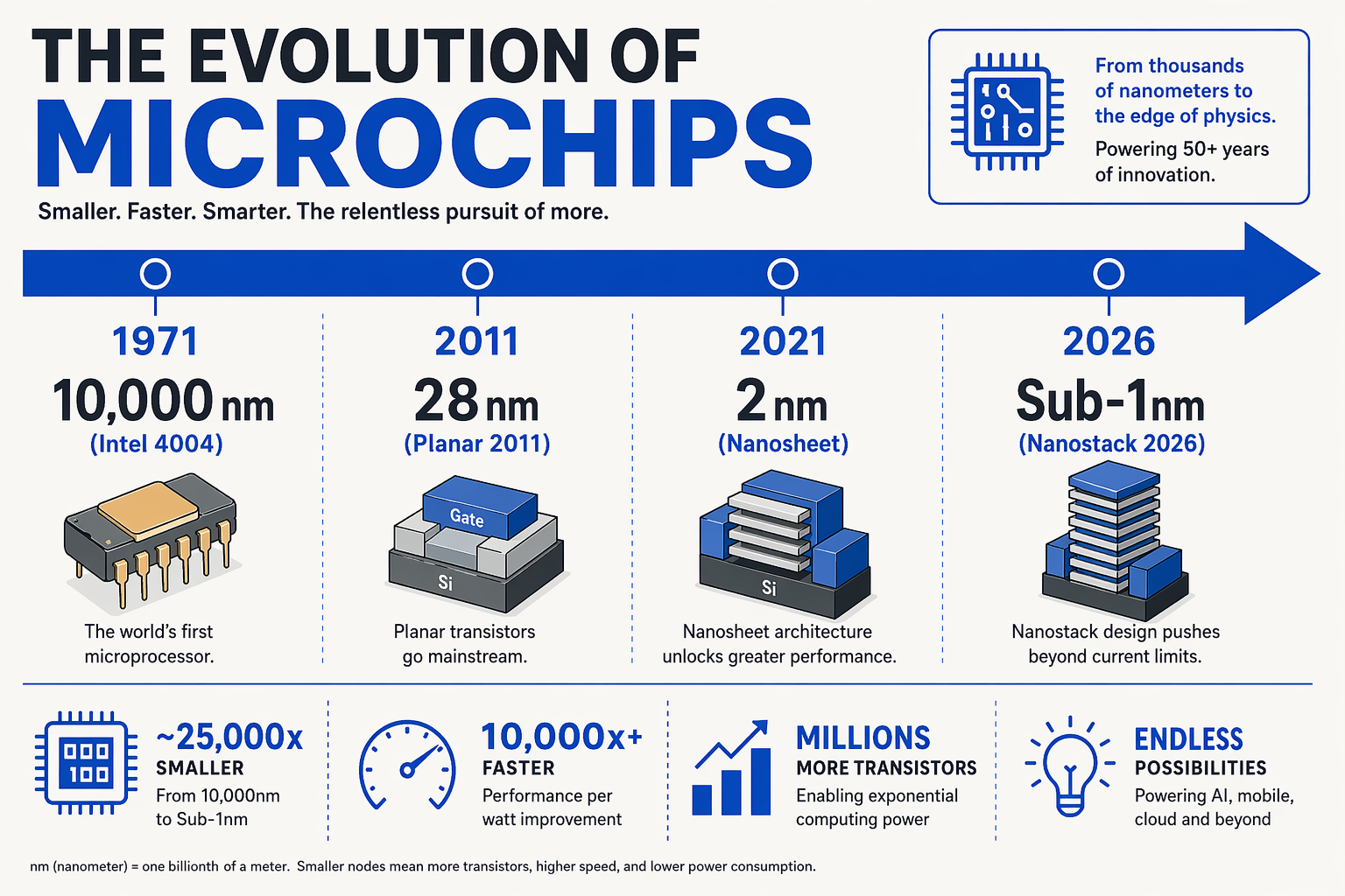
The launch of IBM’s world’s first sub-1 nanometer (nm) chip technology in June 2026 is the culmination of over five decades of relentless progress in semiconductor miniaturization. For context, the semiconductor industry has followed Moore’s Law since the 1960s—the observation that transistor counts on a chip roughly double every two years—though this pace had begun to slow in recent years due to physical and fabrication challenges.
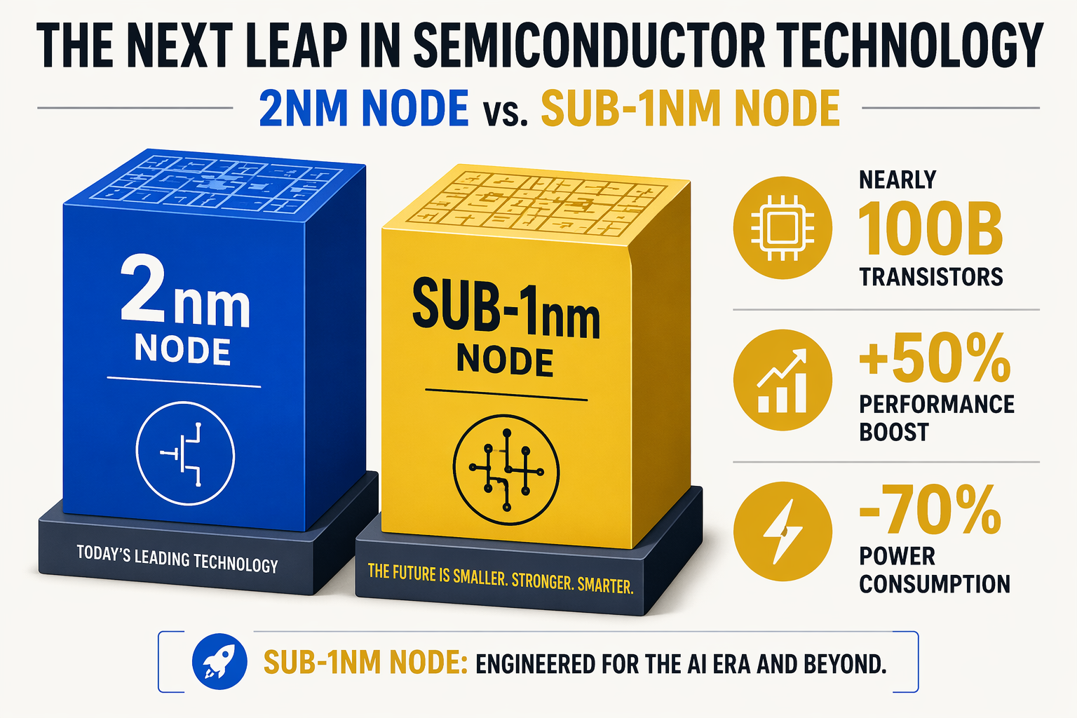
In 1971, Intel’s 4004 processor debuted as the world’s first programmable microchip, with just 2,300 transistors and a process size of 10,000nm [3]. Fast-forward to 2021, IBM announced a 2nm chip technology that could cram 50 billion transistors onto a fingernail-sized chip. Now, just five years later, their sub-1 nm “nanostack” architecture doubles that density to nearly 100 billion transistors on the same footprint [1][8].
Why Sub-1 nm Matters
The sub-1 nm leap represents far more than just another shrink in node size. At these atomic scales, classical 2D transistor designs suffer from quantum tunneling and power leakage, threatening both efficiency and reliability. IBM’s revolutionary “nanostack” 3D architecture addresses these limits by vertically stacking transistors and optimizing atomic layouts, which:
- Increases computational density without proportional growth in heat output
- Enables up to 50% more performance or 70% better energy efficiency compared to the previous node [4]
- Opens the door for new classes of ultra-compact, high-performance AI processors, edge devices, and data center hardware
The Competitive Landscape
IBM’s announcement sets a new industry benchmark, surpassing previous advancements by TSMC, Samsung, and Intel, all of which had set roadmaps to reach 2nm by 2025 but have yet to unveil sub-1 nm production-grade silicon. As of June 2026, IBM stands alone in demonstrating this capability at scale.
- Current industry leaders: TSMC, Samsung, Intel (leading but lagging behind on sub-1 nm)
- Innovation focus: 3D transistor stacking, material science breakthroughs, extreme ultraviolet (EUV) lithography
- Race to commercialization: With nearly 100 billion transistors per chip, the potential impact spans cloud infrastructure, mobile computing, IoT, and advanced AI accelerators
Setting the Stage for the Next Decade
This milestone hints at the new possibilities for industries dependent on AI, high-throughput communications, and real-time analytics. The rise of compute-intensive workloads—from generative AI to 5G/6G core networks—demands ever more power-efficient silicon. In this sense, platforms like CallMissed have a vested interest; for example, deploying multilingual LLM inference or production-grade AI voice agents at scale relies on continual advances in chip density and energy efficiency. As more businesses build on AI communication infrastructure, the need for high-performance, energy-sipping chips will only grow.
IBM’s debut of the sub-1 nm chip not only pushes the semiconductor boundary but also ignites the next chapter of global computing innovation. With its “nanostack” 3D architecture, the industry moves closer to realizing the vision of truly ubiquitous, intelligent, and sustainable technology.
Key Developments (TABLE)
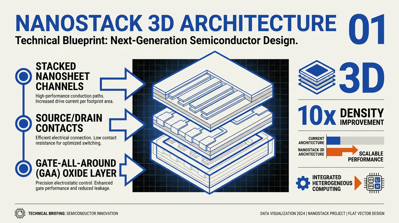
To appreciate the magnitude of IBM’s sub-1 nanometer (nm) breakthrough, one must look at the physical and architectural shifts that made it possible. At the heart of this historic leap is IBM’s revolutionary "nanostack" 3D chip architecture. For decades, the semiconductor industry relied on shrinking 2D planar transistors. As physical limitations loomed, the industry transitioned to FinFET and then to nanosheet designs. IBM's sub-1 nm technology leapfrogs these paradigms by stacking transistors vertically, effectively opening a third dimension for silicon scaling.
This architectural shift allows IBM to pack nearly 100 billion transistors onto a chip the size of a human fingernail. This represents nearly twice the density of IBM's previous 2 nm milestone, offering a clear roadmap for semiconductor innovation over the next decade.
The table below outlines how this new technology compares to previous semiconductor benchmarks:
| Chip Generation | Est. Node | Primary Architecture | Transistor Density (Fingernail Size) | Key Performance Advantage |
|---|---|---|---|---|
| Intel 4004 (1971) | 10,000 nm | Planar (2D) | 2,300 (Total chip count) | Baseline for microprocessing |
| Industry Standard | 28 nm | Planar / 2D | ~100 to 500 Million | Standard legacy computing |
| IBM 2 Nanometer | 2 nm | Nanosheet (GAA) | ~50 Billion | +45% Perf or -75% Energy (vs 7nm) |
| IBM Sub-1 Nanometer | Sub-1 nm | 3D Nanostack | ~100 Billion | +50% Perf or -70% Energy (vs 2nm) |
The Physics of the 3D Nanostack
In traditional chip designs, electrons travel along flat channels. As these channels shrink below 2 nm, quantum tunneling often causes power leakage and signal degradation. IBM’s 3D nanostack architecture mitigates these challenges by vertically stacking nanosheets, allowing for:
- Superior Electrostatic Control: Gate-all-around (GAA) design surrounds the channel on all sides, minimizing current leakage.
- Unprecedented Density: Doubling the transistor count to 100 billion without increasing the physical footprint.
- Design Flexibility: Chip designers can choose between optimizing for extreme speed or ultra-low power consumption, delivering up to 50% more performance or 70% better energy efficiency.
Powering the Next Era of AI Infrastructure
The sheer computational power and efficiency offered by sub-1 nm chips will directly impact the cost and capability of next-generation software. High-density silicon is critical for running massive AI workloads locally and in the cloud.
For instance, communication platforms like CallMissed rely on low-latency, high-throughput systems to process complex tasks—such as translating Speech-to-Text across 22 Indian languages or managing automated AI voice agents. By reducing energy consumption by up to 70%, sub-1 nm technology will make deploying sophisticated, multi-model AI infrastructure commercially viable at an unprecedented global scale, removing the massive power bottlenecks currently facing global data centers.
In-Depth Analysis
The transition to sub-1 nanometer (nm) technology marks a paradigm shift in semiconductor engineering. At these atomic scales, conventional silicon manufacturing processes face extreme quantum limitations, such as electron leakage. To bypass these physical barriers, IBM introduced a revolutionary "nanostack" 3D chip architecture. This approach transitions scaling from a horizontal, planar layout to a vertical stacking methodology, effectively redesigning how transistors interact on a microscopic level and extending the runway for Moore's Law for the next decade.
Quantifying the Performance and Efficiency Gains
By stacking transistors vertically, IBM’s sub-1 nm chip architecture achieves a transistor density that was previously deemed mathematically and physically impossible. It packs nearly 100 billion transistors onto a single piece of silicon no larger than a human fingernail. This represents nearly double the density of IBM’s landmark 2 nm chip.
According to IBM's technical specifications, this dramatic increase in density translates to two distinct operating modes depending on system requirements:
- Maximum Performance Mode: Offers up to a 50% increase in processing performance compared to existing market standards at equivalent power levels.
- Maximum Efficiency Mode: Delivers a massive 70% reduction in energy consumption while maintaining identical performance benchmarks.
To put this historic milestone into perspective, consider the trajectory of computing. The historic Intel 4004 microchip, released over five decades ago, operated on a 10,000 nm node and contained just 2,300 transistors. IBM’s sub-1 nm architecture increases that transistor count by a factor of over 43 million within a fraction of the physical space, fundamentally altering the economics of compute.
Empowering Next-Gen AI and Enterprise Infrastructure
The real-world implications of this breakthrough stretch far beyond raw benchmarks. The global rise of AI has triggered an unprecedented surge in data center power demands. High-density, energy-efficient chips are no longer a luxury; they are an operational necessity for running complex deep learning models, natural language processing (NLP), and agentic workflows at scale.
As this advanced silicon begins to power next-generation cloud infrastructure, AI communication platforms will experience a massive leap in capability. For instance, infrastructure providers like CallMissed—which coordinates real-time Speech-to-Text APIs across 22 regional Indian languages and hosts an API gateway supporting over 300 LLMs—will be able to process highly complex, multi-layered voice and text conversational agents with near-zero latency. Lowering energy requirements by 70% means enterprise-grade AI agents can handle millions of concurrent customer interactions globally without straining the grid or inflating operational overhead.
Impact & Implications

Massive Leap in Computational Power
IBM’s unveiling of the world’s first sub-1 nanometer chip technology represents a watershed moment for the semiconductor industry. Boasting nearly 100 billion transistors on a fingernail-sized chip—almost double the density of IBM’s previous 2nm technology—this advancement is set to redefine the limits of processing power (IBM Newsroom, 2026). The increase in transistor density enables chips to deliver up to 50% more performance or 70% greater energy efficiency compared to current leading-edge designs (X.com source). These gains create ripple effects across sectors reliant on computing, from AI and data centers to consumer electronics and telecommunications.
Energy Efficiency & Sustainability
One of the most significant implications of sub-1 nm technology lies in addressing the industry’s mounting concerns around energy consumption. Large-scale data centers already account for approximately 1-2% of global electricity use (IEA, 2024), with AI workloads causing this number to climb rapidly. IBM’s nanostack architecture—an innovation in 3D chip stacking—can drastically curb these demands:
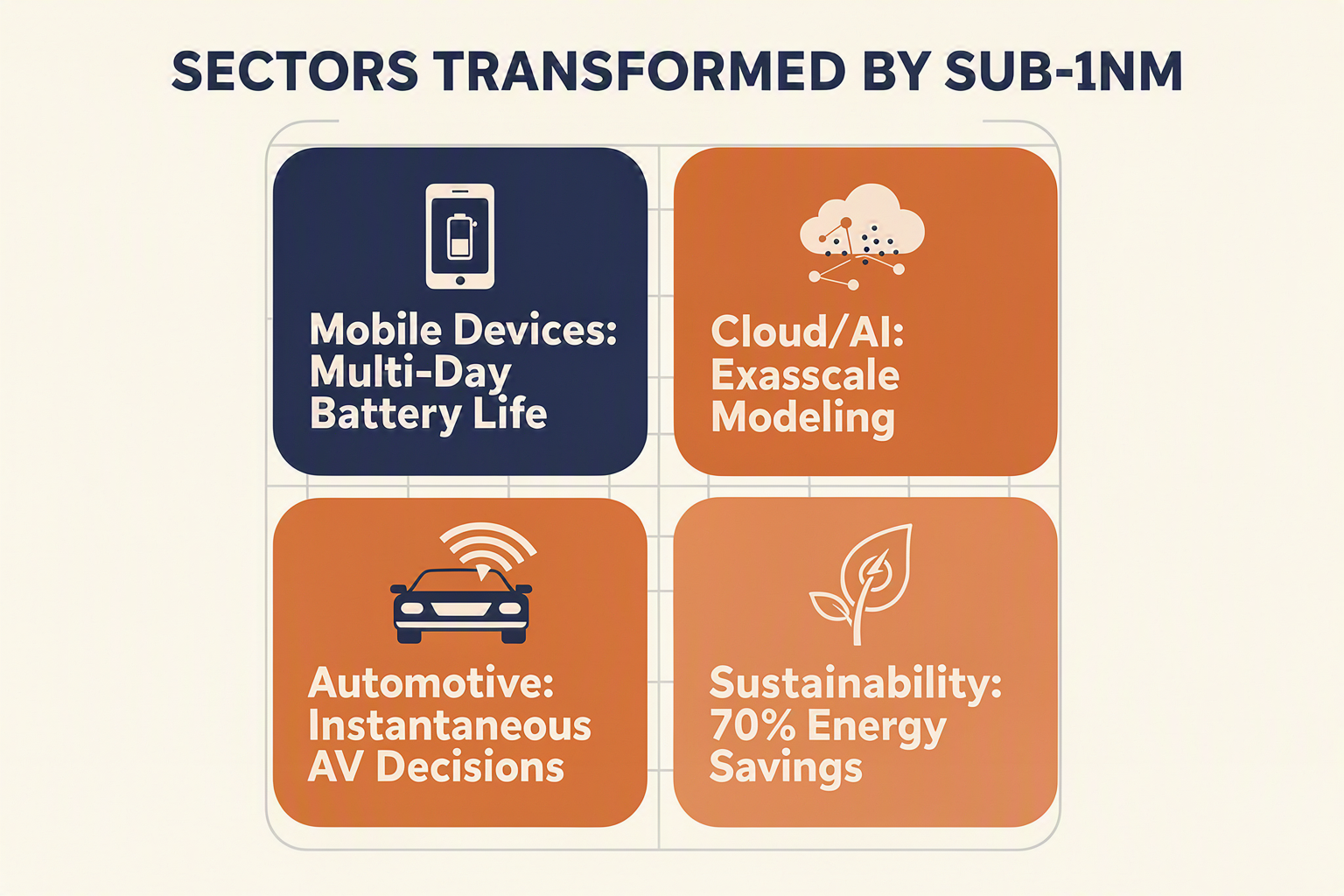
- Up to 70% better energy efficiency versus current chips, prolonging battery life in mobile devices and reducing operational costs and carbon footprints for hyperscale data centers
- Higher computing throughput per watt, enabling power-hungry tasks like LLM inference and real-time analytics to be run on sustainable hardware
Enabling Next-Gen AI & Edge Applications
With nearly 100 billion transistors at its disposal, sub-1 nm chips pave the way for both larger and more efficient AI models. Tasks such as real-time voice synthesis, language translation, and large-scale machine learning inference stand to benefit from:
- Lower latency: Mission-critical edge applications—autonomous vehicles, augmented reality, or IoT nodes—can process data locally at unprecedented speeds
- Smaller form factors: Advanced performance now fits into ultra-portable and embedded devices, removing the historic trade-off between speed and size
- Increased model complexity: AI models with hundreds of billions of parameters can be deployed more broadly, transforming industries like healthcare diagnostics, automotive, and smart city infrastructure
Platforms like CallMissed are already at the forefront of leveraging such breakthroughs—offering LLM inference across 300+ models and deploying AI communication agents capable of serving millions of users in real time. The improved compute power and energy efficiency offered by IBM’s latest chips will help platforms like CallMissed expand multilingual speech-to-text and voice AI capabilities across more devices and edge endpoints.
Shifting Global Semiconductor Dynamics
Historically, each generational leap in chip technology has reshaped global supply chains, R&D investment, and national technology strategies. IBM’s sub-1 nm achievement may accelerate:
- New manufacturing ecosystems: Countries and companies will compete for access to sub-1 nm foundries, spurring further investment in local fabrication and talent pools
- R&D priorities: Focus shifts from classic planar scaling to innovative 3D nanostack architectures, requiring new tooling, materials, and design paradigms
According to industry analysts, the commercial deployment of sub-1 nm chips could power the next decade of exponential growth. As Sandip Patel, IBM India’s Managing Director, remarked, “This is not just a small step, but a giant leap for the future of computing and semiconductor innovation” (LinkedIn source).
Broader Implications & Future Frontiers
From enabling more accessible supercomputing to accelerating breakthroughs in AI-driven healthcare, climate modeling, and scientific research, the impact of sub-1 nm technology will be felt well beyond Silicon Valley. Early adopters among cloud providers, AI platform vendors, and telecom infrastructure builders stand to benefit most—but the entire digital economy is primed for transformation.
In summary, with IBM’s announcement, the semiconductor roadmap has taken an audacious new turn. Emerging platforms—like CallMissed with its focus on scalable, multilingual AI communications—are well-positioned to capitalize on the unprecedented capabilities brought by sub-1 nm chips, redefining the boundaries of what’s possible in the AI-powered era.
Expert Opinions

Industry Leaders Weigh In
IBM’s breakthrough in sub-1 nanometer chip fabrication has ignited strong reactions across the technology sector. Dr. Lisa Su, CEO of AMD, remarked, “This milestone underscores how 3D nanoscale innovation—led by architectures like IBM’s ‘nanostack’—will drive semiconductor capabilities for the next decade.” The ability to pack nearly 100 billion transistors onto a chip the size of a fingernail, as highlighted in IBM’s announcement, marks more than just a technical leap; it signals a seismic shift in what’s possible for computing power and efficiency (IBM newsroom).
Arvind Krishna, Chairman and CEO of IBM, emphasized the importance of these gains: “Our sub-1 nm chip can deliver up to 50% more performance or 70% better energy efficiency compared to our previous 2 nm node.” This has profound implications for data centers and mobile devices, where power constraints and thermal management pose persistent challenges.
Academic and Independent Perspectives
Academic experts are similarly awed, but underline the challenges ahead. Dr. Kaushik Roy, John A. Edwardson Professor of Engineering at Purdue University, explained, “IBM’s nanostack approach could set the tone for future 3D integration, but fabrication at this scale will require new metrology tools, materials science breakthroughs, and rigorous validation.”
Industry analysts echo these sentiments. According to Gartner’s June 2026 semiconductor report, “Transistor density increases of this magnitude—nearly double compared to IBM’s 2 nm generation—may allow artificial intelligence workloads, including model inference and voice synthesis, to run locally at speeds previously only possible via cloud infrastructure.”
Practical Impacts and Concerns
While the excitement is palpable, experts have pointed to practical hurdles:
- Yield and Cost: Manufacturing chips at sub-nanometer nodes could initially suffer from low yields. As a point of reference, TSMC’s early 3 nm processes saw yields below 70%. Analysts expect IBM’s early sub-1 nm yields to be even lower, especially during the ramp-up phase.
- Equipment and Standards: Existing lithography equipment, even extreme ultraviolet (EUV), will need upgrades to handle such tight tolerances.
- Scaling Software: Software optimization is now vital to leverage the full capabilities of these denser chips. As platforms like CallMissed harness increasingly powerful AI infrastructure, support for 300+ models or real-time speech-to-text in 22 Indian languages will become feasible—not just in the cloud, but also at the edge.
Forward-Looking Insights
Nvidia’s CTO Michael Kagan observed, “The significance isn’t just in density or speed—it’s in expanding the economic viability of AI everywhere, from enterprise inference to consumer devices.” This aligns with the global push to democratize advanced computing; for example, Indian startups like CallMissed—leveraging production-ready AI communication infrastructure—stand to directly benefit from the new hardware’s improved efficiency.
For the next decade, a consensus is forming: IBM’s sub-1 nm chips will not merely extend Moore’s Law but may redefine it, opening doors for AI, IoT, and HPC applications previously held back by hardware limitations. As one VC analyst put it on Hacker News, “This is what the semiconductor ‘race to zero’ looks like. Whoever solves the scaling, yield, and energy efficiency puzzle first—wins the next era of tech.”
In sum, IBM’s debut has cemented its role as a technology bellwether, while sparking both optimism and caution among those tasked with turning its promise into real-world impact.
What This Means For You (TABLE)
The transition to sub-1 nanometer technology is not just an incremental upgrade for hardware enthusiasts; it represents a tectonic shift in how we build, deploy, and interact with digital services. By moving beyond traditional planar structures and embracing a groundbreaking 3D "nanostack" architecture, IBM has solved one of the most pressing physical bottlenecks in modern computing.
For enterprises and everyday consumers alike, this hardware revolution translates directly into two massive, selectable benefits: a 50% performance increase or a 70% reduction in energy consumption compared to previous 2 nm technologies. This means devices can either run twice as fast or last up to three times longer on a single charge.
To understand the magnitude of this achievement, we can look at how semiconductor technology has evolved over the decades, leading up to this sub-1 nm breakthrough:
| Technology Node | Transistor Count (Fingernail Size) | Performance vs. Prior Gen | Energy Efficiency | Primary Use Case |
|---|---|---|---|---|
| Intel 4004 (10,000 nm) | ~2,300 transistors | Baseline | High consumption | Primitive, basic calculators |
| Planar Node (28 nm) | ~300 to 500 million | Standard scaling | Moderate efficiency | Early smartphones and PCs |
| IBM 2 nm (2021) | ~50 billion | +45% speed (vs. 7 nm) | 75% reduction (vs. 7 nm) | Modern cloud and flagship mobile SoC |
| IBM Sub-1 nm (2026) | Nearly 100 billion | +50% speed (vs. 2 nm) | 70% reduction (vs. 2 nm) | Generative AI, edge models, quantum-adjacent |
Unlocking the Future of AI and Cloud Infrastructure
For businesses driving the AI revolution, the implications of a sub-1 nm chip are staggering. Today, running massive large language models (LLMs) and real-time voice synthesis demands an immense amount of power and cooling. Scaling down to sub-1 nm means cloud data centers can double their processing capacity without expanding their physical or carbon footprint.
This hardware leap directly supercharges software capabilities. Platforms like CallMissed, which provide cutting-edge AI communication infrastructure, stand to benefit immensely. As chip density increases and energy costs plummet, deploying low-latency AI voice agents, real-time Speech-to-Text APIs supporting 22 regional Indian languages, and complex LLM routing (across 300+ models) will become significantly faster and more cost-effective.
Decentralized "Edge" AI
Furthermore, a 70% reduction in power consumption means we are moving closer to a world where highly complex AI models run locally on consumer devices rather than relying solely on the cloud:
- Smarter Devices: Smartphones and IoT devices will run local, fully conversational AI agents natively without draining their batteries in minutes.
- Hyper-Localized Systems: Businesses can deploy decentralized AI communication agents at the edge, offering unmatched privacy and speed.
- Sustainable Tech: The global carbon footprint of data centers—currently a major environmental concern—could finally begin to plateau even as AI demand skyrockets.
With IBM’s sub-1 nm milestone paving the way for the next decade of semiconductor advancement, the boundaries between hardware limitations and software potential are rapidly dissolving.
Frequently Asked Questions
What is IBM’s sub-1 nanometer chip technology and why is it significant?
How does IBM’s sub-1 nm chip compare to the previous 2 nm technology?
What is the “nanostack” 3D chip architecture featured in IBM’s sub-1 nm chip?
What are the potential applications of IBM’s sub-1 nanometer chip?
When will IBM’s sub-1 nm chips be available for commercial devices and what are production challenges?
How does IBM’s achievement impact the global semiconductor race and what does it mean for AI infrastructure?
Conclusion
IBM’s June 2026 announcement of the world’s first sub-1 nanometer chip technology signals a monumental shift, shattering historical physical scaling limits. Key takeaways include:
- Unprecedented Density: Using a revolutionary "nanostack" 3D architecture, it packs nearly 100 billion transistors onto a fingernail-sized footprint.
- Massive Efficiency Gains: It delivers up to 50% higher performance or a staggering 70% reduction in energy consumption compared to previous nodes.
- The Future of Compute: It establishes a highly efficient hardware foundation to power the next decade of compute-heavy AI development.
Looking forward, watch for how this hyper-efficient silicon decentralizes AI, bringing massive LLMs directly onto localized edge devices without draining power grids. As hardware capabilities scale exponentially, forward-thinking businesses must adapt their software strategies to match. To explore how AI communication is already evolving to leverage these breakthroughs, check out CallMissed—an AI infrastructure platform powering high-performance, real-time voice agents and multilingual chatbots.
As the physical foundation of computing is rewritten, how will your organization harness the power of hyper-efficient AI?
Related Posts

Meta Loses 20 Million Users Across WhatsApp, Instagram, and Facebook: What It Means for Q1 2026 and Beyond

Kunal Shah to Lead WhatsApp: 9 Indian-Origin CEOs Driving Global Tech Leadership

India Seeks New Semiconductor Investments at Global Tech Summit: What It Means for the Future